0.60dellt110
dellt110 时间:2021-03-26 阅读:()
DocumentNumber:91127www.
vishay.
comS10-2466-Rev.
C,25-Oct-101PowerMOSFETIRFD110,SiHFD110VishaySiliconixFEATURESDynamicdV/dtRatingRepetitiveAvalancheRatedForAutomaticInsertionEndStackable175°COperatingTemperatureFastSwitchingandEaseofParallelingComplianttoRoHSDirective2002/95/ECDESCRIPTIONThirdgenerationPowerMOSFETsfromVishayprovidethedesignerwiththebestcombinationoffastswitching,ruggedizeddevicedesign,lowon-resistanceandcost-effectiveness.
The4pinDIPpackageisalowcostmachine-insertablecasestylewhichcanbestackedinmultiplecombinationsonstandard0.
1"pincenters.
Thedualdrainservesasathermallinktothemountingsurfaceforpowerdissipationlevelsupto1W.
Notesa.
Repetitiverating;pulsewidthlimitedbymaximumjunctiontemperature(seefig.
11).
b.
VDD=25V,startingTJ=25°C,L=52mH,Rg=25,IAS=2.
0A(seefig.
12).
c.
ISD5.
6A,dI/dt75A/μs,VDDVDS,TJ175°C.
d.
1.
6mmfromcase.
PRODUCTSUMMARYVDS(V)100RDS(on)()VGS=10V0.
54Qg(Max.
)(nC)8.
3Qgs(nC)2.
3Qgd(nC)3.
8ConfigurationSingleN-ChannelMOSFETGDSHVMDIPDSGAvailableRoHS*COMPLIANTORDERINGINFORMATIONPackageHVMDIPLead(Pb)-freeIRFD110PbFSiHFD110-E3SnPbIRFD110SiHFD110ABSOLUTEMAXIMUMRATINGS(TA=25°C,unlessotherwisenoted)PARAMETERSYMBOLLIMITUNITDrain-SourceVoltageVDS100VGate-SourceVoltageVGS±20ContinuousDrainCurrentVGSat10VTA=25°CID1.
0ATA=100°C0.
71PulsedDrainCurrentaIDM8.
0LinearDeratingFactor0.
0083W/°CSinglePulseAvalancheEnergybEAS140mJRepetitiveAvalancheCurrentaIAR1.
0ARepetitiveAvalancheEnergyaEAR0.
13mJMaximumPowerDissipationTA=25°CPD1.
3WPeakDiodeRecoverydV/dtcdV/dt5.
5V/nsOperatingJunctionandStorageTemperatureRangeTJ,Tstg-55to+175°CSolderingRecommendations(PeakTemperature)for10s300d*PbcontainingterminationsarenotRoHScompliant,exemptionsmayapplywww.
vishay.
comDocumentNumber:911272S10-2466-Rev.
C,25-Oct-10IRFD110,SiHFD110VishaySiliconixNotesa.
Repetitiverating;pulsewidthlimitedbymaximumjunctiontemperature(seefig.
11).
b.
Pulsewidth300μs;dutycycle2%.
THERMALRESISTANCERATINGSPARAMETERSYMBOLTYP.
MAX.
UNITMaximumJunction-to-AmbientRthJA-120°C/WSPECIFICATIONS(TJ=25°C,unlessotherwisenoted)PARAMETERSYMBOLTESTCONDITIONSMIN.
TYP.
MAX.
UNITStaticDrain-SourceBreakdownVoltageVDSVGS=0V,ID=250μA100--VVDSTemperatureCoefficientVDS/TJReferenceto25°C,ID=1mA-0.
12-V/°CGate-SourceThresholdVoltageVGS(th)VDS=VGS,ID=250μA2.
0-4.
0VGate-SourceLeakageIGSSVGS=±20V--±100nAZeroGateVoltageDrainCurrentIDSSVDS=100V,VGS=0V--25μAVDS=80V,VGS=0V,TJ=150°C--250Drain-SourceOn-StateResistanceRDS(on)VGS=10VID=0.
60Ab--0.
54ForwardTransconductancegfsVDS=50V,ID=0.
60Ab0.
80--SDynamicInputCapacitanceCissVGS=0V,VDS=25V,f=1.
0MHz,seefig.
5-180-pFOutputCapacitanceCoss-81-ReverseTransferCapacitanceCrss-15-TotalGateChargeQgVGS=10VID=5.
6A,VDS=80V,seefig.
6and13b--8.
3nCGate-SourceChargeQgs--2.
3Gate-DrainChargeQgd--3.
8Turn-OnDelayTimetd(on)VDD=50V,ID=5.
6A,Rg=24,RD=8.
4,seefig.
10b-6.
9-nsRiseTimetr-16-Turn-OffDelayTimetd(off)-15-FallTimetf-9.
4-InternalDrainInductanceLDBetweenlead,6mm(0.
25")frompackageandcenterofdiecontact-4.
0-nHInternalSourceInductanceLS-6.
0-Drain-SourceBodyDiodeCharacteristicsContinuousSource-DrainDiodeCurrentISMOSFETsymbolshowingtheintegralreversep-njunctiondiode--1.
0APulsedDiodeForwardCurrentaISM--8.
0BodyDiodeVoltageVSDTJ=25°C,IS=1.
0A,VGS=0Vb--2.
5VBodyDiodeReverseRecoveryTimetrrTJ=25°C,IF=5.
6A,dI/dt=100A/μsb-100200nsBodyDiodeReverseRecoveryChargeQrr-0.
440.
88μCForwardTurn-OnTimetonIntrinsicturn-ontimeisnegligible(turn-onisdominatedbyLSandLD)DSGSDGDocumentNumber:91127www.
vishay.
comS10-2466-Rev.
C,25-Oct-103IRFD110,SiHFD110VishaySiliconixTYPICALCHARACTERISTICS(25°C,unlessotherwisenoted)Fig.
1-TypicalOutputCharacteristics,TA=25°CFig.
2-TypicalOutputCharacteristics,TA=175°CFig.
3-TypicalTransferCharacteristicsFig.
4-NormalizedOn-Resistancevs.
Temperature91127_0120sPulseWidthTA=25°C4.
5VVDS,Drain-to-SourceVoltage(V)ID,DrainCurrent(A)BottomTopVGS15V10V8.
0V7.
0V6.
0V5.
5V5.
0V4.
5V10110010010110-191127_0210110010010110-1BottomTopVGS15V10V8.
0V7.
0V6.
0V5.
5V5.
0V4.
5V20sPulseWidthTA=175°C4.
5VVDS,Drain-to-SourceVoltage(V)ID,DrainCurrent(A)91127_03101100ID,DrainCurrent(A)VGS,Gate-to-SourceVoltage(V)5678910410-125°C175°C20sPulseWidthVDS=50V91127_04ID=5.
6AVGS=10V3.
00.
00.
51.
01.
52.
02.
5-60-40-20020406080100120140160TJ,JunctionTemperature(°C)RDS(on),Drain-to-SourceOnResistance(Normalized)180www.
vishay.
comDocumentNumber:911274S10-2466-Rev.
C,25-Oct-10IRFD110,SiHFD110VishaySiliconixFig.
5-TypicalCapacitancevs.
Drain-to-SourceVoltageFig.
6-TypicalGateChargevs.
Gate-to-SourceVoltageFig.
7-TypicalSource-DrainDiodeForwardVoltageFig.
8-MaximumSafeOperatingArea91127_05400320240160080100101Capacitance(pF)VDS,Drain-to-SourceVoltage(V)VGS=0V,f=1MHzCiss=Cgs+Cgd,CdsShortedCrss=CgdCoss=Cds+CgdCissCrssCoss91127_06QG,TotalGateCharge(nC)VGS,Gate-to-SourceVoltage(V)20161280402864ID=5.
6AVDS=20VFortestcircuitseefigure1310VDS=50VVDS=80V91127_0725°C175°CVGS=0V10-1100VSD,Source-to-DrainVoltage(V)ISD,ReverseDrainCurrent(A)0.
50.
90.
80.
70.
61.
01.
21.
191127_08ID,DrainCurrent(A)102252525VDS,Drain-to-SourceVoltage(V)1101022525250.
11100.
12510310s100s1ms10msOperationinthisarealimitedbyRDS(on)TA=25°CTJ=175°CSinglePulseDocumentNumber:91127www.
vishay.
comS10-2466-Rev.
C,25-Oct-105IRFD110,SiHFD110VishaySiliconixFig.
9-MaximumDrainCurrentvs.
AmbientTemperatureFig.
10a-SwitchingTimeTestCircuitFig.
10b-SwitchingTimeWaveformsFig.
11-MaximumEffectiveTransientThermalImpedance,Junction-to-Ambient91127_09ID,DrainCurrent(A)TA,AmbientTemperature(°C)0.
00.
20.
40.
80.
62515012510075501751.
0Pulsewidth≤1sDutyfactor≤0.
1%RDVGSRgD.
U.
T.
10V+-VDSVDDVDS90%10%VGStd(on)trtd(off)tf91127_110-0.
50.
20.
10.
050.
01SinglePulse(ThermalResponse)PDMt1t2Notes:1.
DutyFactor,D=t1/t22.
PeakTj=PDMxZthJC+TC0.
02ThermalResponse(ZthJA)t1,RectangularPulseDuration(s)10-510-410-310-20.
111010210310.
110-210210103www.
vishay.
comDocumentNumber:911276S10-2466-Rev.
C,25-Oct-10IRFD110,SiHFD110VishaySiliconixFig.
12a-UnclampedInductiveTestCircuitFig.
12b-UnclampedInductiveWaveformsFig.
12c-MaximumAvalancheEnergyvs.
DrainCurrentFig.
13a-BasicGateChargeWaveformFig.
13b-GateChargeTestCircuitRgIAS0.
01WtpD.
U.
T.
LVDS+-VDD10VVarytptoobtainrequiredIASIASVDSVDDVDStp91127_12c050100200300350251501251007550StartingTJ,JunctionTemperature(°C)EAS,SinglePulseEnergy(mJ)BottomTopID0.
82A1.
4A2.
0AVDD=25V175150250QGSQGDQGVGCharge10VD.
U.
T.
3mAVGSVDSIGID0.
3F0.
2F50kΩ12VCurrentregulatorCurrentsamplingresistorsSametypeasD.
U.
T.
+-DocumentNumber:91127www.
vishay.
comS10-2466-Rev.
C,25-Oct-107IRFD110,SiHFD110VishaySiliconixFig.
14-ForN-ChannelVishaySiliconixmaintainsworldwidemanufacturingcapability.
Productsmaybemanufacturedatoneofseveralqualifiedlocations.
ReliabilitydataforSiliconTechnologyandPackageReliabilityrepresentacompositeofallqualifiedlocations.
Forrelateddocumentssuchaspackage/tapedrawings,partmarking,andreliabilitydata,seewww.
vishay.
com/ppg91127.
P.
W.
PerioddI/dtDioderecoverydV/dtRipple≤5%BodydiodeforwarddropRe-appliedvoltageReverserecoverycurrentBodydiodeforwardcurrentVGS=10VaISDDrivergatedriveD.
U.
T.
lSDwaveformD.
U.
T.
VDSwaveformInductorcurrentD=P.
W.
Period+-+++---PeakDiodeRecoverydV/dtTestCircuitVDDdV/dtcontrolledbyRgDriversametypeasD.
U.
T.
ISDcontrolledbydutyfactor"D"D.
U.
T.
-deviceundertestD.
U.
T.
CircuitlayoutconsiderationsLowstrayinductanceGroundplaneLowleakageinductancecurrenttransformerRgNotea.
VGS=5VforlogicleveldevicesVDDDocumentNumber:91361www.
vishay.
comRevision:06-Sep-101PackageInformationVishaySiliconixHVMDIP(Highvoltage)Note1.
Packagelengthdoesnotincludemoldflash,protrusionsorgateburrs.
Packagewidthdoesnotincludeinterleadflashorprotrusions.
INCHESMILLIMETERSDIM.
MIN.
MAX.
MIN.
MAX.
A0.
3100.
3307.
878.
38E0.
3000.
4257.
6210.
79L0.
2700.
2906.
867.
36ECN:X10-0386-Rev.
B,06-Sep-10DWG:59740.
248[6.
29]0.
240[6.
10]0.
197[5.
00]0.
189[4.
80]0.
024[0.
60]0.
020[0.
51]0.
160[4.
06]0.
140[3.
56]0.
180[4.
57]0.
160[4.
06]4x0.
100[2.
54]typ.
AL0.
045[1.
14]0.
035[0.
89]2x0.
043[1.
09]0.
035[0.
89]0.
094[2.
38]0.
086[2.
18]0.
017[0.
43]0.
013[0.
33]0°to15°2xEmin.
Emax.
0.
133[3.
37]0.
125[3.
18]LegalDisclaimerNoticewww.
vishay.
comVishayRevision:01-Jan-20211DocumentNumber:91000DisclaimerALLPRODUCT,PRODUCTSPECIFICATIONSANDDATAARESUBJECTTOCHANGEWITHOUTNOTICETOIMPROVERELIABILITY,FUNCTIONORDESIGNOROTHERWISE.
VishayIntertechnology,Inc.
,itsaffiliates,agents,andemployees,andallpersonsactingonitsortheirbehalf(collectively,"Vishay"),disclaimanyandallliabilityforanyerrors,inaccuraciesorincompletenesscontainedinanydatasheetorinanyotherdisclosurerelatingtoanyproduct.
Vishaymakesnowarranty,representationorguaranteeregardingthesuitabilityoftheproductsforanyparticularpurposeorthecontinuingproductionofanyproduct.
Tothemaximumextentpermittedbyapplicablelaw,Vishaydisclaims(i)anyandallliabilityarisingoutoftheapplicationoruseofanyproduct,(ii)anyandallliability,includingwithoutlimitationspecial,consequentialorincidentaldamages,and(iii)anyandallimpliedwarranties,includingwarrantiesoffitnessforparticularpurpose,non-infringementandmerchantability.
StatementsregardingthesuitabilityofproductsforcertaintypesofapplicationsarebasedonVishay'sknowledgeoftypicalrequirementsthatareoftenplacedonVishayproductsingenericapplications.
Suchstatementsarenotbindingstatementsaboutthesuitabilityofproductsforaparticularapplication.
Itisthecustomer'sresponsibilitytovalidatethataparticularproductwiththepropertiesdescribedintheproductspecificationissuitableforuseinaparticularapplication.
Parametersprovidedindatasheetsand/orspecificationsmayvaryindifferentapplicationsandperformancemayvaryovertime.
Alloperatingparameters,includingtypicalparameters,mustbevalidatedforeachcustomerapplicationbythecustomer'stechnicalexperts.
ProductspecificationsdonotexpandorotherwisemodifyVishay'stermsandconditionsofpurchase,includingbutnotlimitedtothewarrantyexpressedtherein.
Exceptasexpresslyindicatedinwriting,Vishayproductsarenotdesignedforuseinmedical,life-saving,orlife-sustainingapplicationsorforanyotherapplicationinwhichthefailureoftheVishayproductcouldresultinpersonalinjuryordeath.
CustomersusingorsellingVishayproductsnotexpresslyindicatedforuseinsuchapplicationsdosoattheirownrisk.
PleasecontactauthorizedVishaypersonneltoobtainwrittentermsandconditionsregardingproductsdesignedforsuchapplications.
Nolicense,expressorimplied,byestoppelorotherwise,toanyintellectualpropertyrightsisgrantedbythisdocumentorbyanyconductofVishay.
Productnamesandmarkingsnotedhereinmaybetrademarksoftheirrespectiveowners.
2021VISHAYINTERTECHNOLOGY,INC.
ALLRIGHTSRESERVED
vishay.
comS10-2466-Rev.
C,25-Oct-101PowerMOSFETIRFD110,SiHFD110VishaySiliconixFEATURESDynamicdV/dtRatingRepetitiveAvalancheRatedForAutomaticInsertionEndStackable175°COperatingTemperatureFastSwitchingandEaseofParallelingComplianttoRoHSDirective2002/95/ECDESCRIPTIONThirdgenerationPowerMOSFETsfromVishayprovidethedesignerwiththebestcombinationoffastswitching,ruggedizeddevicedesign,lowon-resistanceandcost-effectiveness.
The4pinDIPpackageisalowcostmachine-insertablecasestylewhichcanbestackedinmultiplecombinationsonstandard0.
1"pincenters.
Thedualdrainservesasathermallinktothemountingsurfaceforpowerdissipationlevelsupto1W.
Notesa.
Repetitiverating;pulsewidthlimitedbymaximumjunctiontemperature(seefig.
11).
b.
VDD=25V,startingTJ=25°C,L=52mH,Rg=25,IAS=2.
0A(seefig.
12).
c.
ISD5.
6A,dI/dt75A/μs,VDDVDS,TJ175°C.
d.
1.
6mmfromcase.
PRODUCTSUMMARYVDS(V)100RDS(on)()VGS=10V0.
54Qg(Max.
)(nC)8.
3Qgs(nC)2.
3Qgd(nC)3.
8ConfigurationSingleN-ChannelMOSFETGDSHVMDIPDSGAvailableRoHS*COMPLIANTORDERINGINFORMATIONPackageHVMDIPLead(Pb)-freeIRFD110PbFSiHFD110-E3SnPbIRFD110SiHFD110ABSOLUTEMAXIMUMRATINGS(TA=25°C,unlessotherwisenoted)PARAMETERSYMBOLLIMITUNITDrain-SourceVoltageVDS100VGate-SourceVoltageVGS±20ContinuousDrainCurrentVGSat10VTA=25°CID1.
0ATA=100°C0.
71PulsedDrainCurrentaIDM8.
0LinearDeratingFactor0.
0083W/°CSinglePulseAvalancheEnergybEAS140mJRepetitiveAvalancheCurrentaIAR1.
0ARepetitiveAvalancheEnergyaEAR0.
13mJMaximumPowerDissipationTA=25°CPD1.
3WPeakDiodeRecoverydV/dtcdV/dt5.
5V/nsOperatingJunctionandStorageTemperatureRangeTJ,Tstg-55to+175°CSolderingRecommendations(PeakTemperature)for10s300d*PbcontainingterminationsarenotRoHScompliant,exemptionsmayapplywww.
vishay.
comDocumentNumber:911272S10-2466-Rev.
C,25-Oct-10IRFD110,SiHFD110VishaySiliconixNotesa.
Repetitiverating;pulsewidthlimitedbymaximumjunctiontemperature(seefig.
11).
b.
Pulsewidth300μs;dutycycle2%.
THERMALRESISTANCERATINGSPARAMETERSYMBOLTYP.
MAX.
UNITMaximumJunction-to-AmbientRthJA-120°C/WSPECIFICATIONS(TJ=25°C,unlessotherwisenoted)PARAMETERSYMBOLTESTCONDITIONSMIN.
TYP.
MAX.
UNITStaticDrain-SourceBreakdownVoltageVDSVGS=0V,ID=250μA100--VVDSTemperatureCoefficientVDS/TJReferenceto25°C,ID=1mA-0.
12-V/°CGate-SourceThresholdVoltageVGS(th)VDS=VGS,ID=250μA2.
0-4.
0VGate-SourceLeakageIGSSVGS=±20V--±100nAZeroGateVoltageDrainCurrentIDSSVDS=100V,VGS=0V--25μAVDS=80V,VGS=0V,TJ=150°C--250Drain-SourceOn-StateResistanceRDS(on)VGS=10VID=0.
60Ab--0.
54ForwardTransconductancegfsVDS=50V,ID=0.
60Ab0.
80--SDynamicInputCapacitanceCissVGS=0V,VDS=25V,f=1.
0MHz,seefig.
5-180-pFOutputCapacitanceCoss-81-ReverseTransferCapacitanceCrss-15-TotalGateChargeQgVGS=10VID=5.
6A,VDS=80V,seefig.
6and13b--8.
3nCGate-SourceChargeQgs--2.
3Gate-DrainChargeQgd--3.
8Turn-OnDelayTimetd(on)VDD=50V,ID=5.
6A,Rg=24,RD=8.
4,seefig.
10b-6.
9-nsRiseTimetr-16-Turn-OffDelayTimetd(off)-15-FallTimetf-9.
4-InternalDrainInductanceLDBetweenlead,6mm(0.
25")frompackageandcenterofdiecontact-4.
0-nHInternalSourceInductanceLS-6.
0-Drain-SourceBodyDiodeCharacteristicsContinuousSource-DrainDiodeCurrentISMOSFETsymbolshowingtheintegralreversep-njunctiondiode--1.
0APulsedDiodeForwardCurrentaISM--8.
0BodyDiodeVoltageVSDTJ=25°C,IS=1.
0A,VGS=0Vb--2.
5VBodyDiodeReverseRecoveryTimetrrTJ=25°C,IF=5.
6A,dI/dt=100A/μsb-100200nsBodyDiodeReverseRecoveryChargeQrr-0.
440.
88μCForwardTurn-OnTimetonIntrinsicturn-ontimeisnegligible(turn-onisdominatedbyLSandLD)DSGSDGDocumentNumber:91127www.
vishay.
comS10-2466-Rev.
C,25-Oct-103IRFD110,SiHFD110VishaySiliconixTYPICALCHARACTERISTICS(25°C,unlessotherwisenoted)Fig.
1-TypicalOutputCharacteristics,TA=25°CFig.
2-TypicalOutputCharacteristics,TA=175°CFig.
3-TypicalTransferCharacteristicsFig.
4-NormalizedOn-Resistancevs.
Temperature91127_0120sPulseWidthTA=25°C4.
5VVDS,Drain-to-SourceVoltage(V)ID,DrainCurrent(A)BottomTopVGS15V10V8.
0V7.
0V6.
0V5.
5V5.
0V4.
5V10110010010110-191127_0210110010010110-1BottomTopVGS15V10V8.
0V7.
0V6.
0V5.
5V5.
0V4.
5V20sPulseWidthTA=175°C4.
5VVDS,Drain-to-SourceVoltage(V)ID,DrainCurrent(A)91127_03101100ID,DrainCurrent(A)VGS,Gate-to-SourceVoltage(V)5678910410-125°C175°C20sPulseWidthVDS=50V91127_04ID=5.
6AVGS=10V3.
00.
00.
51.
01.
52.
02.
5-60-40-20020406080100120140160TJ,JunctionTemperature(°C)RDS(on),Drain-to-SourceOnResistance(Normalized)180www.
vishay.
comDocumentNumber:911274S10-2466-Rev.
C,25-Oct-10IRFD110,SiHFD110VishaySiliconixFig.
5-TypicalCapacitancevs.
Drain-to-SourceVoltageFig.
6-TypicalGateChargevs.
Gate-to-SourceVoltageFig.
7-TypicalSource-DrainDiodeForwardVoltageFig.
8-MaximumSafeOperatingArea91127_05400320240160080100101Capacitance(pF)VDS,Drain-to-SourceVoltage(V)VGS=0V,f=1MHzCiss=Cgs+Cgd,CdsShortedCrss=CgdCoss=Cds+CgdCissCrssCoss91127_06QG,TotalGateCharge(nC)VGS,Gate-to-SourceVoltage(V)20161280402864ID=5.
6AVDS=20VFortestcircuitseefigure1310VDS=50VVDS=80V91127_0725°C175°CVGS=0V10-1100VSD,Source-to-DrainVoltage(V)ISD,ReverseDrainCurrent(A)0.
50.
90.
80.
70.
61.
01.
21.
191127_08ID,DrainCurrent(A)102252525VDS,Drain-to-SourceVoltage(V)1101022525250.
11100.
12510310s100s1ms10msOperationinthisarealimitedbyRDS(on)TA=25°CTJ=175°CSinglePulseDocumentNumber:91127www.
vishay.
comS10-2466-Rev.
C,25-Oct-105IRFD110,SiHFD110VishaySiliconixFig.
9-MaximumDrainCurrentvs.
AmbientTemperatureFig.
10a-SwitchingTimeTestCircuitFig.
10b-SwitchingTimeWaveformsFig.
11-MaximumEffectiveTransientThermalImpedance,Junction-to-Ambient91127_09ID,DrainCurrent(A)TA,AmbientTemperature(°C)0.
00.
20.
40.
80.
62515012510075501751.
0Pulsewidth≤1sDutyfactor≤0.
1%RDVGSRgD.
U.
T.
10V+-VDSVDDVDS90%10%VGStd(on)trtd(off)tf91127_110-0.
50.
20.
10.
050.
01SinglePulse(ThermalResponse)PDMt1t2Notes:1.
DutyFactor,D=t1/t22.
PeakTj=PDMxZthJC+TC0.
02ThermalResponse(ZthJA)t1,RectangularPulseDuration(s)10-510-410-310-20.
111010210310.
110-210210103www.
vishay.
comDocumentNumber:911276S10-2466-Rev.
C,25-Oct-10IRFD110,SiHFD110VishaySiliconixFig.
12a-UnclampedInductiveTestCircuitFig.
12b-UnclampedInductiveWaveformsFig.
12c-MaximumAvalancheEnergyvs.
DrainCurrentFig.
13a-BasicGateChargeWaveformFig.
13b-GateChargeTestCircuitRgIAS0.
01WtpD.
U.
T.
LVDS+-VDD10VVarytptoobtainrequiredIASIASVDSVDDVDStp91127_12c050100200300350251501251007550StartingTJ,JunctionTemperature(°C)EAS,SinglePulseEnergy(mJ)BottomTopID0.
82A1.
4A2.
0AVDD=25V175150250QGSQGDQGVGCharge10VD.
U.
T.
3mAVGSVDSIGID0.
3F0.
2F50kΩ12VCurrentregulatorCurrentsamplingresistorsSametypeasD.
U.
T.
+-DocumentNumber:91127www.
vishay.
comS10-2466-Rev.
C,25-Oct-107IRFD110,SiHFD110VishaySiliconixFig.
14-ForN-ChannelVishaySiliconixmaintainsworldwidemanufacturingcapability.
Productsmaybemanufacturedatoneofseveralqualifiedlocations.
ReliabilitydataforSiliconTechnologyandPackageReliabilityrepresentacompositeofallqualifiedlocations.
Forrelateddocumentssuchaspackage/tapedrawings,partmarking,andreliabilitydata,seewww.
vishay.
com/ppg91127.
P.
W.
PerioddI/dtDioderecoverydV/dtRipple≤5%BodydiodeforwarddropRe-appliedvoltageReverserecoverycurrentBodydiodeforwardcurrentVGS=10VaISDDrivergatedriveD.
U.
T.
lSDwaveformD.
U.
T.
VDSwaveformInductorcurrentD=P.
W.
Period+-+++---PeakDiodeRecoverydV/dtTestCircuitVDDdV/dtcontrolledbyRgDriversametypeasD.
U.
T.
ISDcontrolledbydutyfactor"D"D.
U.
T.
-deviceundertestD.
U.
T.
CircuitlayoutconsiderationsLowstrayinductanceGroundplaneLowleakageinductancecurrenttransformerRgNotea.
VGS=5VforlogicleveldevicesVDDDocumentNumber:91361www.
vishay.
comRevision:06-Sep-101PackageInformationVishaySiliconixHVMDIP(Highvoltage)Note1.
Packagelengthdoesnotincludemoldflash,protrusionsorgateburrs.
Packagewidthdoesnotincludeinterleadflashorprotrusions.
INCHESMILLIMETERSDIM.
MIN.
MAX.
MIN.
MAX.
A0.
3100.
3307.
878.
38E0.
3000.
4257.
6210.
79L0.
2700.
2906.
867.
36ECN:X10-0386-Rev.
B,06-Sep-10DWG:59740.
248[6.
29]0.
240[6.
10]0.
197[5.
00]0.
189[4.
80]0.
024[0.
60]0.
020[0.
51]0.
160[4.
06]0.
140[3.
56]0.
180[4.
57]0.
160[4.
06]4x0.
100[2.
54]typ.
AL0.
045[1.
14]0.
035[0.
89]2x0.
043[1.
09]0.
035[0.
89]0.
094[2.
38]0.
086[2.
18]0.
017[0.
43]0.
013[0.
33]0°to15°2xEmin.
Emax.
0.
133[3.
37]0.
125[3.
18]LegalDisclaimerNoticewww.
vishay.
comVishayRevision:01-Jan-20211DocumentNumber:91000DisclaimerALLPRODUCT,PRODUCTSPECIFICATIONSANDDATAARESUBJECTTOCHANGEWITHOUTNOTICETOIMPROVERELIABILITY,FUNCTIONORDESIGNOROTHERWISE.
VishayIntertechnology,Inc.
,itsaffiliates,agents,andemployees,andallpersonsactingonitsortheirbehalf(collectively,"Vishay"),disclaimanyandallliabilityforanyerrors,inaccuraciesorincompletenesscontainedinanydatasheetorinanyotherdisclosurerelatingtoanyproduct.
Vishaymakesnowarranty,representationorguaranteeregardingthesuitabilityoftheproductsforanyparticularpurposeorthecontinuingproductionofanyproduct.
Tothemaximumextentpermittedbyapplicablelaw,Vishaydisclaims(i)anyandallliabilityarisingoutoftheapplicationoruseofanyproduct,(ii)anyandallliability,includingwithoutlimitationspecial,consequentialorincidentaldamages,and(iii)anyandallimpliedwarranties,includingwarrantiesoffitnessforparticularpurpose,non-infringementandmerchantability.
StatementsregardingthesuitabilityofproductsforcertaintypesofapplicationsarebasedonVishay'sknowledgeoftypicalrequirementsthatareoftenplacedonVishayproductsingenericapplications.
Suchstatementsarenotbindingstatementsaboutthesuitabilityofproductsforaparticularapplication.
Itisthecustomer'sresponsibilitytovalidatethataparticularproductwiththepropertiesdescribedintheproductspecificationissuitableforuseinaparticularapplication.
Parametersprovidedindatasheetsand/orspecificationsmayvaryindifferentapplicationsandperformancemayvaryovertime.
Alloperatingparameters,includingtypicalparameters,mustbevalidatedforeachcustomerapplicationbythecustomer'stechnicalexperts.
ProductspecificationsdonotexpandorotherwisemodifyVishay'stermsandconditionsofpurchase,includingbutnotlimitedtothewarrantyexpressedtherein.
Exceptasexpresslyindicatedinwriting,Vishayproductsarenotdesignedforuseinmedical,life-saving,orlife-sustainingapplicationsorforanyotherapplicationinwhichthefailureoftheVishayproductcouldresultinpersonalinjuryordeath.
CustomersusingorsellingVishayproductsnotexpresslyindicatedforuseinsuchapplicationsdosoattheirownrisk.
PleasecontactauthorizedVishaypersonneltoobtainwrittentermsandconditionsregardingproductsdesignedforsuchapplications.
Nolicense,expressorimplied,byestoppelorotherwise,toanyintellectualpropertyrightsisgrantedbythisdocumentorbyanyconductofVishay.
Productnamesandmarkingsnotedhereinmaybetrademarksoftheirrespectiveowners.
2021VISHAYINTERTECHNOLOGY,INC.
ALLRIGHTSRESERVED
简单测评v5.net的美国cn2云服务器:电信双程cn2+联通AS9929+移动直连
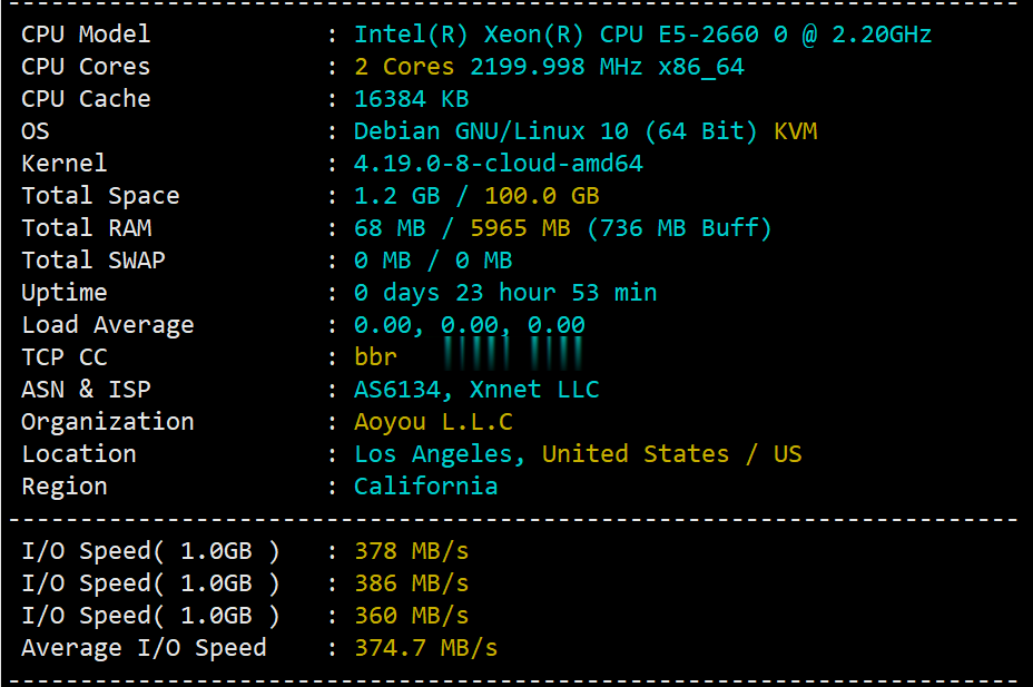
v5.net一直做独立服务器这块儿的,自从推出云服务器(VPS)以来站长一直还没有关注过,在网友的提醒下弄了个6G内存、2核、100G SSD的美国云服务器来写测评,主机测评给大家趟雷,让你知道v5.net的美国云服务器效果怎么样。本次测评数据仅供参考,有兴趣的还是亲自测试吧! 官方网站:https://v5.net/cloud.html 从显示来看CPU是e5-2660(2.2GHz主频),...
Megalayer 香港CN2优化线路VPS主机速度和性能综合评测
对于Megalayer云服务器提供商在之前也有对于他们家的美国服务器和香港服务器进行过评测和介绍,但是对于大部分网友来说需要独立服务器和站群服务器并不是特别的普及,我们很多网友使用较多的还是云服务器或者VPS主机比较多。在前面也有在"Megalayer新增香港VPS主机 1GB内存 50GB SSD 2M带宽 月59元"文章中有介绍到Megalayer商家有新增香港CN2优化VPS主机。那时候看这...

咖啡主机22元/月起,美国洛杉矶弹性轻量云主机仅13元/月起,高防云20G防御仅18元/月
咖啡主机怎么样?咖啡主机是一家国人主机销售商,成立于2016年8月,之前云服务器网已经多次分享过他家的云服务器产品了,商家主要销售香港、洛杉矶等地的VPS产品,Cera机房 三网直连去程 回程CUVIP优化 本产品并非原生地区本土IP,线路方面都有CN2直连国内,机器比较稳定。咖啡主机目前推出美国洛杉矶弹性轻量云主机仅13元/月起,高防云20G防御仅18元/月;香港弹性云服务器,香港HKBN CN...

dellt110为你推荐
-
对对塔今儿老师给推荐了一个叫对对塔的学习网站,看起来挺不错的,有用过的人吗?管不管用?哪些功能比较好啊?网红名字被抢注谁知道这个网红叫什么名字?求帮助!22zizi.com河南福利彩票22选52010175开奖结果百度关键词分析百度竞价关键词分析需要从哪些数据入手?百度指数词什么是百度指数广告法新修订的《广告法》有哪些内容www.hyyan.comdota屠夫怎么玩?从初期到后期的装备是什么?机器蜘蛛挑战或是生存Boss是一只巨型机器蜘蛛的第一人称射击游戏叫什么www.gogo.com哪种丰胸产品是不含激素的?汴京清谈汴京繁华 简介50字?