analysiswww.sesezy.com
www.sesezy.com 时间:2021-03-18 阅读:()
ADC121S021www.
ti.
comSNAS305G–JULY2005–REVISEDJANUARY2010ADC121S021SingleChannel,50to200ksps,12-BitA/DConverterCheckforSamples:ADC121S0211FEATURESDESCRIPTIONTheADC121S021isalow-power,singlechannel23SpecifiedOveraRangeofSampleRates.
CMOS12-bitanalog-to-digitalconverterwithahigh-6-LeadWSONandSOT-23Packagesspeedserialinterface.
UnliketheconventionalVariablePowerManagementpracticeofspecifyingperformanceatasinglesamplerateonly,theADC121S021isfullyspecifiedoveraSinglePowerSupplywith2.
7V-5.
25VRangesampleraterangeof50kspsto200ksps.
TheSPI/QSPI/MICROWIRE/DSPCompatibleconverterisbaseduponasuccessive-approximationregisterarchitecturewithaninternaltrack-and-holdAPPLICATIONScircuit.
PortableSystemsTheoutputserialdataisstraightbinary,andisRemoteDataAcquisitioncompatiblewithseveralstandards,suchasSPI,QSPI,MICROWIRE,andmanycommonDSPInstrumentationandControlSystemsserialinterfaces.
TheADC121S021operateswithasinglesupplythatcanrangefrom+2.
7Vto+5.
25V.
Normalpowerconsumptionusinga+3.
6Vor+5.
25Vsupplyis1.
5mWand7.
9mW,respectively.
Thepower-downfeaturereducesthepowerconsumptiontoaslowas2.
6Wusinga+5.
25Vsupply.
TheADC121S021ispackagedin6-leadWSONandSOT-23packages.
Operationovertheindustrialtemperaturerangeof40°Cto+85°Cisguaranteed.
Table1.
KeySpecificationsVALUEUNITDNL+0.
45/-0.
25LSB(typ)INL+0.
45/-0.
4LSB(typ)SNR72.
3dB(typ)3.
6VSupply1.
5mW(typ)PowerConsumption5.
25VSupply7.
9mW(typ)Table2.
Pin-CompatibleAlternativesbyResolutionandSpeed(1)SpecifiedforSampleRateRangeof:Resolution50to200ksps200to500ksps500kspsto1Msps12-bitADC121S021ADC121S051ADC121S10110-bitADC101S021ADC101S051ADC101S1018-bitADC081S021ADC081S051ADC081S101(1)Alldevicesarefullypinandfunctioncompatible.
1Pleasebeawarethatanimportantnoticeconcerningavailability,standardwarranty,anduseincriticalapplicationsofTexasInstrumentssemiconductorproductsanddisclaimerstheretoappearsattheendofthisdatasheet.
2TRI-STATEisaregisteredtrademarkofTexasInstruments.
3Allothertrademarksarethepropertyoftheirrespectiveowners.
PRODUCTIONDATAinformationiscurrentasofpublicationdate.
Copyright2005–2010,TexasInstrumentsIncorporatedProductsconformtospecificationsperthetermsoftheTexasInstrumentsstandardwarranty.
Productionprocessingdoesnotnecessarilyincludetestingofallparameters.
ADC121S021SNAS305G–JULY2005–REVISEDJANUARY2010www.
ti.
comConnectionDiagramFigure1.
WSONorSOT-23PackageSeePackageNumbersNGF0006A,DBV0006ABlockDiagramPinDescriptionsPinNo.
NameDescriptionANALOGI/O3VINAnaloginput.
Thissignalcanrangefrom0VtoVA.
DIGITALI/O4SCLKDigitalclockinput.
Thisclockdirectlycontrolstheconversionandreadoutprocesses.
5SDATADigitaldataoutput.
TheoutputsamplesareclockedoutofthispinonfallingedgesoftheSCLKpin.
6CSChipselect.
OnthefallingedgeofCS,aconversionprocessbegins.
POWERSUPPLYPositivesupplypin.
Thispinshouldbeconnectedtoaquiet+2.
7Vto+5.
25Vsourceandbypassedto1VAGNDwitha1Fcapacitoranda0.
1Fmonolithiccapacitorlocatedwithin1cmofthepowerpin.
2GNDThegroundreturnforthesupplyandsignals.
ForpackagesuffixCISD(X)only,itisrecommendedthatthecenterpadshouldbeconnectedtoPADGNDground.
Thesedeviceshavelimitedbuilt-inESDprotection.
TheleadsshouldbeshortedtogetherorthedeviceplacedinconductivefoamduringstorageorhandlingtopreventelectrostaticdamagetotheMOSgates.
2SubmitDocumentationFeedbackCopyright2005–2010,TexasInstrumentsIncorporatedProductFolderLinks:ADC121S021ADC121S021www.
ti.
comSNAS305G–JULY2005–REVISEDJANUARY2010AbsoluteMaximumRatings(1)(2)(3)AnalogSupplyVoltageVA0.
3Vto6.
5VVoltageonAnyDigitalPintoGND0.
3Vto6.
5VVoltageonAnyAnalogPintoGND0.
3Vto(VA+0.
3V)InputCurrentatAnyPin(4)±10mAPackageInputCurrent(4)±20mAPowerConsumptionatTA=25°CSee(5)ESDSusceptibility(6)HumanBodyModel3500VMachineModel300VJunctionTemperature+150°CStorageTemperature65°Cto+150°C(1)AbsoluteMaximumRatingsindicatelimitsbeyondwhichdamagetothedevicemayoccur.
OperatingRatingsindicateconditionsforwhichthedeviceisfunctional,butdonotguaranteespecificperformancelimits.
Forguaranteedspecificationsandtestconditions,seetheElectricalCharacteristics.
Theguaranteedspecificationsapplyonlyforthetestconditionslisted.
Someperformancecharacteristicsmaydegradewhenthedeviceisnotoperatedunderthelistedtestconditions.
(2)AllvoltagesaremeasuredwithrespecttoGND=0V,unlessotherwisespecified.
(3)IfMilitary/Aerospacespecifieddevicesarerequired,pleasecontacttheTISalesOffice/Distributorsforavailabilityandspecifications.
(4)Whentheinputvoltageatanypinexceedsthepowersupply(thatis,VINVA),thecurrentatthatpinshouldbelimitedto10mA.
The20mAmaximumpackageinputcurrentratinglimitsthenumberofpinsthatcansafelyexceedthepowersupplieswithaninputcurrentof10mAtotwo.
TheAbsoluteMaximumRatingspecificationdoesnotapplytotheVApin.
ThecurrentintotheVApinislimitedbytheAnalogSupplyVoltagespecification.
(5)Theabsolutemaximumjunctiontemperature(TJmax)forthisdeviceis150°C.
ThemaximumallowablepowerdissipationisdictatedbyTJmax,thejunction-to-ambientthermalresistance(θJA),andtheambienttemperature(TA),andcanbecalculatedusingtheformulaPDmax=(TJmaxTA)/θJA.
Thevaluesformaximumpowerdissipationlistedabovewillbereachedonlywhenthedeviceisoperatedinaseverefaultcondition(e.
g.
wheninputoroutputpinsaredrivenbeyondthepowersupplyvoltages,orthepowersupplypolarityisreversed).
Obviously,suchconditionsshouldalwaysbeavoided.
(6)Humanbodymodelis100pFcapacitordischargedthrougha1.
5kresistor.
Machinemodelis220pFdischargedthroughzeroohmsOperatingRatings(1)(2)OperatingTemperatureRange40°C≤TA≤+85°CVASupplyVoltage+2.
7Vto+5.
25VDigitalInputPinsVoltageRange0.
3Vto+5.
25V(regardlessofsupplyvoltage)AnalogInputPinsVoltageRange0VtoVAClockFrequency25kHzto20MHzSampleRateupto1Msps(1)AbsoluteMaximumRatingsindicatelimitsbeyondwhichdamagetothedevicemayoccur.
OperatingRatingsindicateconditionsforwhichthedeviceisfunctional,butdonotguaranteespecificperformancelimits.
Forguaranteedspecificationsandtestconditions,seetheElectricalCharacteristics.
Theguaranteedspecificationsapplyonlyforthetestconditionslisted.
Someperformancecharacteristicsmaydegradewhenthedeviceisnotoperatedunderthelistedtestconditions.
(2)AllvoltagesaremeasuredwithrespecttoGND=0V,unlessotherwisespecified.
PackageThermalResistance(1)PackageθJA6-leadWSON94°C/W6-leadSOT-23265°C/W(1)SolderingprocessmustcomplywithNationalSemiconductor'sReflowTemperatureProfilespecifications.
Refertowww.
national.
com/packaging.
()Copyright2005–2010,TexasInstrumentsIncorporatedSubmitDocumentationFeedback3ProductFolderLinks:ADC121S021ADC121S021SNAS305G–JULY2005–REVISEDJANUARY2010www.
ti.
comADC121S021ConverterElectricalCharacteristics(1)(2)ThefollowingspecificationsapplyforVA=+2.
7Vto5.
25V,fSCLK=1MHzto4MHz,fSAMPLE=50kspsto200ksps,CL=15pF,unlessotherwisenoted.
BoldfacelimitsapplyforTA=TMINtoTMAX:allotherlimitsTA=25°C.
LimitsParameterTestConditionsTypicalUnits(2)STATICCONVERTERCHARACTERISTICSResolutionwithNoMissingCodes12Bits+0.
45LSB(max)VA=+2.
7Vto+3.
6V±1.
00.
40LSB(min)INLIntegralNon-Linearity+0.
55LSB(max)VA=+4.
75vto+5.
25V0.
40LSB(min)+0.
45+1.
0LSB(max)VA=+2.
7Vto+3.
6V0.
250.
8LSB(min)DNLDifferentialNon-Linearity+0.
60LSB(max)VA=+4.
75vto+5.
25V0.
30LSB(min)VA=+2.
7vto+3.
6V0.
18±1.
2VOFFOffsetErrorLSB(max)VA=+4.
75vto+5.
25V0.
26VA=+2.
7to+3.
6V0.
75±1.
5GEGainErrorLSB(max)VA=+4.
75vto+5.
25V1.
6DYNAMICCONVERTERCHARACTERISTICSVA=+2.
7to5.
25VSINADSignal-to-NoisePlusDistortionRatio7270dBFS(min)fIN=100kHz,0.
02dBFSVA=+2.
7to5.
25VSNRSignal-to-NoiseRatio72.
370.
8dBFS(min)fIN=100kHz,0.
02dBFSVA=+2.
7to5.
25VTHDTotalHarmonicDistortion83dBFSfIN=100kHz,0.
02dBFSVA=+2.
7to5.
25VSFDRSpurious-FreeDynamicRange85dBfIN=100kHz,0.
02dBFSVA=+2.
7to5.
25VENOBEffectiveNumberofBits11.
711.
3Bits(min)fIN=100kHz,0.
02dBFSIntermodulationDistortion,SecondVA=+5.
25V83dBFSOrderTermsfa=103.
5kHz,fb=113.
5kHzIMDIntermodulationDistortion,ThirdOrderVA=+5.
25V82dBFSTermsfa=103.
5kHz,fb=113.
5kHzVA=+5V11MHzFPBW-3dBFullPowerBandwidthVA=+3V8MHzANALOGINPUTCHARACTERISTICSVINInputRange0toVAVIDCLDCLeakageCurrent±1A(max)TrackMode30pFCINAInputCapacitanceHoldMode4pFDIGITALINPUTCHARACTERISTICSVA=+5.
25V2.
4V(min)VIHInputHighVoltageVA=+3.
6V2.
1V(min)VA=+5V0.
8V(max)VILInputLowVoltageVA=+3V0.
4V(max)IINInputCurrentVIN=0VorVA±0.
1±1A(max)CINDDigitalInputCapacitance24pF(max)(1)TestedlimitsareguaranteedtoNational'sAOQL(AverageOutgoingQualityLevel).
(2)Datasheetmin/maxspecificationlimitsareguaranteedbydesign,test,orstatisticalanalysis.
4SubmitDocumentationFeedbackCopyright2005–2010,TexasInstrumentsIncorporatedProductFolderLinks:ADC121S021ADC121S021www.
ti.
comSNAS305G–JULY2005–REVISEDJANUARY2010ADC121S021ConverterElectricalCharacteristics(1)(2)(continued)ThefollowingspecificationsapplyforVA=+2.
7Vto5.
25V,fSCLK=1MHzto4MHz,fSAMPLE=50kspsto200ksps,CL=15pF,unlessotherwisenoted.
BoldfacelimitsapplyforTA=TMINtoTMAX:allotherlimitsTA=25°C.
LimitsParameterTestConditionsTypicalUnits(2)DIGITALOUTPUTCHARACTERISTICSISOURCE=200AVA0.
07VA0.
2V(min)VOHOutputHighVoltageISOURCE=1mAVA0.
1VISINK=200A0.
030.
4V(max)VOLOutputLowVoltageISINK=1mA0.
1VIOZH,IOZLTRI-STATELeakageCurrent±0.
1±10A(max)COUTTRI-STATEOutputCapacitance24pF(max)OutputCodingStraight(Natural)BinaryPOWERSUPPLYCHARACTERISTICS2.
7V(min)VASupplyVoltage5.
25V(max)VA=+5.
25V,1.
52.
8mA(max)fSAMPLE=200kspsSupplyCurrent,NormalMode(Operational,CSlow)VA=+3.
6V,0.
401.
2mA(max)fSAMPLE=200kspsIAfSCLK=0MHz,VA=+5.
25V500nAfSAMPLE=0kspsSupplyCurrent,Shutdown(CShigh)VA=+5.
25V,fSCLK=4MHz,60AfSAMPLE=0kspsVA=+5.
25V7.
914.
7mW(max)PowerConsumption,NormalMode(Operational,CSlow)VA=+3.
6V1.
54.
3mW(max)fSCLK=0MHz,VA=+5.
25VPD2.
6WfSAMPLE=0kspsPowerConsumption,Shutdown(CShigh)VA=+5.
25V,fSCLK=4MHz,315WfSAMPLE=0kspsACELECTRICALCHARACTERISTICS1.
0MHz(min)fSCLKClockFrequency(3)4.
0MHz(max)50ksps(min)fSSampleRate(3)200ksps(max)40%(min)DCSCLKDutyCyclefSCLK=4MHz5060%(max)tACQMinimumTimeRequiredforAcquisition350ns(max)tQUIET(4)50ns(min)tADApertureDelay3nstAJApertureJitter30ps(3)Thisisthefrequencyrangeoverwhichtheelectricalperformanceisguaranteed.
ThedeviceisfunctionaloverawiderrangewhichisspecifiedunderOperatingRatings.
(4)MinimumQuietTimerequiredbybusrelinquishandthestartofthenextconversion.
Copyright2005–2010,TexasInstrumentsIncorporatedSubmitDocumentationFeedback5ProductFolderLinks:ADC121S021ADC121S021SNAS305G–JULY2005–REVISEDJANUARY2010www.
ti.
comADC121S021TimingSpecificationsThefollowingspecificationsapplyforVA=+2.
7Vto5.
25V,GND=0V,fSCLK=1.
0MHzto4.
0MHz,CL=25pF,fSAMPLE=50kspsto200ksps,BoldfacelimitsapplyforTA=TMINtoTMAX:allotherlimitsTA=25°C.
ParameterTestConditionsTypicalLimitsUnitstCSMinimumCSPulseWidth10ns(min)tSUCStoSCLKSetupTime10ns(min)tENDelayfromCSUntilSDATATRI-STATEDisabled(1)20ns(max)VA=+2.
7Vto+3.
6V40ns(max)tACCDataAccessTimeafterSCLKFallingEdge(2)VA=+4.
75Vto+5.
25V20ns(max)tCLSCLKLowPulseWidth0.
4xtSCLKns(min)tCHSCLKHighPulseWidth0.
4xtSCLKns(min)VA=+2.
7Vto+3.
6V7ns(min)tHSCLKtoDataValidHoldTimeVA=+4.
75Vto+5.
25V5ns(min)25ns(max)VA=+2.
7Vto+3.
6V6ns(min)tDISSCLKFallingEdgetoSDATAHighImpedance(3)25ns(max)VA=+4.
75Vto+5.
25V5ns(min)tPOWER-UPPower-UpTimefromFullPower-Down1s(1)MeasuredwiththetimingtestcircuitshowninFigure2anddefinedasthetimetakenbytheoutputsignaltocross1.
0V.
(2)MeasuredwiththetimingtestcircuitshowninFigure2anddefinedasthetimetakenbytheoutputsignaltocross1.
0Vor2.
0V.
(3)tDISisderivedfromthetimetakenbytheoutputstochangeby0.
5VwiththetimingtestcircuitshowninFigure2.
Themeasurednumberisthenadjustedtoremovetheeffectsofchargingordischargingtheoutputcapacitance.
ThismeansthattDISisthetruebusrelinquishtime,independentofthebusloading.
TIMINGDIAGRAMSFigure2.
TimingTestCircuit6SubmitDocumentationFeedbackCopyright2005–2010,TexasInstrumentsIncorporatedProductFolderLinks:ADC121S021ADC121S021www.
ti.
comSNAS305G–JULY2005–REVISEDJANUARY2010Figure3.
ADC121S021SerialTimingDiagramSpecificationDefinitionsACQUISITIONTIMEisthetimerequiredtoacquiretheinputvoltage.
Thatis,itistimerequiredfortheholdcapacitortochargeuptotheinputvoltage.
AcquisitiontimeismeasuredbackwardsfromthefallingedgeofCSwhenthesignalissampledandthepartmovesfromtracktohold.
ThestartofthetimeintervalthatcontainsTACQisthe13thrisingedgeofSCLKofthepreviousconversionwhenthepartmovesfromholdtotrack.
Theusermustensurethatthetimebetweenthe13thrisingedgeofSCLKandthefallingedgeofthenextCSisnotlessthanTACQtomeetperformancespecifications.
APERTUREDELAYisthetimeafterthefallingedgeofCStowhentheinputsignalisacquiredorheldforconversion.
APERTUREJITTER(APERTUREUNCERTAINTY)isthevariationinaperturedelayfromsampletosample.
Aperturejittermanifestsitselfasnoiseintheoutput.
CONVERSIONTIMEisthetimerequired,aftertheinputvoltageisacquired,fortheADCtoconverttheinputvoltagetoadigitalword.
ThisisfromthefallingedgeofCSwhentheinputsignalissampledtothe16thfallingedgeofSCLKwhentheSDATAoutputgoesintoTRI-STATE.
DIFFERENTIALNON-LINEARITY(DNL)isthemeasureofthemaximumdeviationfromtheidealstepsizeof1LSB.
DUTYCYCLEistheratioofthetimethatarepetitivedigitalwaveformishightothetotaltimeofoneperiod.
ThespecificationherereferstotheSCLK.
EFFECTIVENUMBEROFBITS(ENOB,orEFFECTIVEBITS)isanothermethodofspecifyingSignal-to-NoiseandDistortionorSINAD.
ENOBisdefinedas(SINAD1.
76)/6.
02andsaysthattheconverterisequivalenttoaperfectADCofthis(ENOB)numberofbits.
FULLPOWERBANDWIDTHisameasureofthefrequencyatwhichthereconstructedoutputfundamentaldrops3dBbelowitslowfrequencyvalueforafullscaleinput.
GAINERRORisthedeviationofthelastcodetransition(111.
.
.
110)to(111.
.
.
111)fromtheideal(VREF1.
5LSB),afteradjustingforoffseterror.
INTEGRALNON-LINEARITY(INL)isameasureofthedeviationofeachindividualcodefromalinedrawnfromnegativefullscale(LSBbelowthefirstcodetransition)throughpositivefullscale(LSBabovethelastcodetransition).
Thedeviationofanygivencodefromthisstraightlineismeasuredfromthecenterofthatcodevalue.
INTERMODULATIONDISTORTION(IMD)isthecreationofadditionalspectralcomponentsasaresultoftwosinusoidalfrequenciesbeingappliedtotheADCinputatthesametime.
Itisdefinedastheratioofthepowerinthesecondandthirdorderintermodulationproductstothesumofthepowerinbothoftheoriginalfrequencies.
IMDisusuallyexpressedindB.
Copyright2005–2010,TexasInstrumentsIncorporatedSubmitDocumentationFeedback7ProductFolderLinks:ADC121S021ADC121S021SNAS305G–JULY2005–REVISEDJANUARY2010www.
ti.
comMISSINGCODESarethoseoutputcodesthatwillneverappearattheADCoutputs.
TheADC121S021isguaranteednottohaveanymissingcodes.
OFFSETERRORisthedeviationofthefirstcodetransition(000.
.
.
000)to(000.
.
.
001)fromtheideal(i.
e.
GND+0.
5LSB).
SIGNALTONOISERATIO(SNR)istheratio,expressedindB,ofthermsvalueoftheinputsignaltothermsvalueofthesumofallotherspectralcomponentsbelowone-halfthesamplingfrequency,notincludingharmonicsord.
c.
SIGNALTONOISEPLUSDISTORTION(S/N+DorSINAD)Istheratio,expressedindB,ofthermsvalueoftheinputsignaltothermsvalueofalloftheotherspectralcomponentsbelowhalftheclockfrequency,includingharmonicsbutexcludingd.
c.
SPURIOUSFREEDYNAMICRANGE(SFDR)isthedifference,expressedindB,betweenthedesiredsignalamplitudetotheamplitudeofthepeakspuriousspectralcomponent,whereaspuriousspectralcomponentisanysignalpresentintheoutputspectrumthatisnotpresentattheinputandmayormaynotbeaharmonic.
TOTALHARMONICDISTORTION(THD)istheratio,expressedindBordBc,ofthermstotalofthefirstfiveharmoniccomponentsattheoutputtothermsleveloftheinputsignalfrequencyasseenattheoutput.
THDiscalculatedas:(1)whereAf1istheRMSpoweroftheinputfrequencyattheoutputandAf2throughAf6aretheRMSpowerinthefirst5harmonicfrequencies.
THROUGHPUTTIMEistheminimumtimerequiredbetweenthestartoftwosuccessiveconversion.
Itistheacquisitiontimeplustheconversiontime.
8SubmitDocumentationFeedbackCopyright2005–2010,TexasInstrumentsIncorporatedProductFolderLinks:ADC121S021ADC121S021www.
ti.
comSNAS305G–JULY2005–REVISEDJANUARY2010TypicalPerformanceCharacteristicsTA=+25°C,fSAMPLE=50kspsto200ksps,fSCLK=1MHzto4MHz,fIN=100kHzunlessotherwisestated.
DNLINLfSCLK=1MHzfSCLK=1MHzFigure4.
Figure5.
DNLINLfSCLK=4MHzfSCLK=4MHzFigure6.
Figure7.
DNLINLvs.
vs.
ClockFrequencyClockFrequencyFigure8.
Figure9.
Copyright2005–2010,TexasInstrumentsIncorporatedSubmitDocumentationFeedback9ProductFolderLinks:ADC121S021ADC121S021SNAS305G–JULY2005–REVISEDJANUARY2010www.
ti.
comTypicalPerformanceCharacteristics(continued)TA=+25°C,fSAMPLE=50kspsto200ksps,fSCLK=1MHzto4MHz,fIN=100kHzunlessotherwisestated.
SNRSINADvs.
vs.
ClockFrequencyClockFrequencyFigure10.
Figure11.
SFDRTHDvs.
vs.
ClockFrequencyClockFrequencyFigure12.
Figure13.
PowerConsumptionvs.
SpectralResponse,VA=5.
25VThroughput,fSCLK=4MHzfSCLK=4MHzFigure14.
Figure15.
10SubmitDocumentationFeedbackCopyright2005–2010,TexasInstrumentsIncorporatedProductFolderLinks:ADC121S021ADC121S021www.
ti.
comSNAS305G–JULY2005–REVISEDJANUARY2010APPLICATIONSINFORMATIONADC121S021OPERATIONTheADC121S021isasuccessive-approximationanalog-to-digitalconverterdesignedaroundacharge-redistributiondigital-to-analogconvertercore.
SimplifiedschematicsoftheADC121S021inbothtrackandholdmodesareshowninFigure16andFigure17,respectively.
InFigure16,thedeviceisintrackmode:switchSW1connectsthesamplingcapacitortotheinput,andSW2balancesthecomparatorinputs.
ThedeviceisinthisstateuntilCSisbroughtlow,atwhichpointthedevicemovestotheholdmode.
Figure17showsthedeviceinholdmode:switchSW1connectsthesamplingcapacitortoground,maintainingthesampledvoltage,andswitchSW2unbalancesthecomparator.
Thecontrollogictheninstructsthecharge-redistributionDACtoaddorsubtractfixedamountsofchargefromthesamplingcapacitoruntilthecomparatorisbalanced.
Whenthecomparatorisbalanced,thedigitalwordsuppliedtotheDACisthedigitalrepresentationoftheanaloginputvoltage.
Thedevicemovesfromholdmodetotrackmodeonthe13thrisingedgeofSCLK.
Figure16.
ADC121S021inTrackModeFigure17.
ADC121S021inHoldModeUSINGTHEADC121S021TheserialinterfacetimingdiagramfortheADCisshowninFigure3.
CSischipselect,whichinitiatesconversionsontheADCandframestheserialdatatransfers.
SCLK(serialclock)controlsboththeconversionprocessandthetimingofserialdata.
SDATAistheserialdataoutpin,whereaconversionresultisfoundasaserialdatastream.
BasicoperationoftheADCbeginswithCSgoinglow,whichinitiatesaconversionprocessanddatatransfer.
SubsequentrisingandfallingedgesofSCLKwillbelabelledwithreferencetothefallingedgeofCS;forexample,"thethirdfallingedgeofSCLK"shallrefertothethirdfallingedgeofSCLKafterCSgoeslow.
AtthefallofCS,theSDATApincomesoutofTRI-STATE,andtheconvertermovesfromtrackmodetoholdmode.
TheinputsignalissampledandheldforconversiononthefallingedgeofCS.
Theconvertermovesfromholdmodetotrackmodeonthe13thrisingedgeofSCLK(seeFigure3).
ItisatthispointthattheintervalfortheTACQspecificationbegins.
Intheworstcase,350nsmustpassbetweenthe13thrisingedgeandthenextfallingedgeofSCLK.
TheSDATApinwillbeplacedbackintoTRI-STATEafterthe16thfallingedgeofSCLK,orattherisingedgeofCS,whicheveroccursfirst.
Afteraconversioniscompleted,thequiettime(tQUIET)mustbesatisfiedbeforebringingCSlowagaintobeginanotherconversion.
Copyright2005–2010,TexasInstrumentsIncorporatedSubmitDocumentationFeedback11ProductFolderLinks:ADC121S021ADC121S021SNAS305G–JULY2005–REVISEDJANUARY2010www.
ti.
comSixteenSCLKcyclesarerequiredtoreadacompletesamplefromtheADC.
Thesamplebits(includingleadingzeroes)areclockedoutonfallingedgesofSCLK,andareintendedtobeclockedinbyareceiveronsubsequentrisingedgesofSCLK.
TheADCwillproducethreeleadingzerobitsonSDATA,followedbytwelvedatabits,mostsignificantfirst.
IfCSgoeslowbeforetherisingedgeofSCLK,anadditional(fourth)zerobitmaybecapturedbythenextfallingedgeofSCLK.
DeterminingThroughputThroughputdependsonthefrequencyofSCLKandhowmuchtimeisallowedtoelapsebetweentheendofoneconversionandthestartofanother.
AtthemaximumspecifiedSCLKfrequency,themaximumguaranteedthroughputisobtainedbyusinga20SCLKframe.
AsshowninFigure3,theminimumallowedtimebetweenCSfallingedgesisdeterminedby1)12.
5SCLKsforHoldmode,2)thelargeroftwoquantities:eithertheminimumrequiredtimeforTrackmode(tACQ)or2.
5SCLKstofinishreadingtheresultand3)0,1/2or1SCLKpaddingtoensureanevennumberofSCLKcyclessothereisafallingSCLKedgewhenCSnextfalls.
Forexample,atthefastestrateforthisfamilyofparts,SCLKis20MHzand2.
5SCLKsare125ns,sotheminimumtimebetweenCSfallingedgesiscalculatedby:12.
5*50ns+350ns+0.
5*50ns=1000ns(2)(12.
5SCLKs+tACQ+1/2SCLK)whichcorrespondstoamaximumthroughputof1MSPS.
Attheslowestrateforthisfamily,SCLKis1MHz.
Usinga20cycleconversionframeasshowninFigure3yieldsa20μstimebetweenCSfallingedgesforathroughputof50KSPS.
Itispossible,however,tousefewerthan20clockcyclesprovidedthetimingparametersaremet.
Witha1MHzSCLK,thereare2500nsin2.
5SCLKcycles,whichisgreaterthantACQ.
Afterthelastdatabithascomeout,theclockwillneedonefullcycletoreturntoafallingedge.
ThusthetotaltimebetweenfallingedgesofCSis12.
5*1μs+2.
5*1μs+1*1μs=16μswhichisathroughputof62.
5KSPS.
ADC121S021TRANSFERFUNCTIONTheoutputformatoftheADCisstraightbinary.
CodetransitionsoccurmidwaybetweensuccessiveintegerLSBvalues.
TheLSBwidthfortheADCisVA/4096.
TheidealtransfercharacteristicisshowninFigure18.
Thetransitionfromanoutputcodeof000000000000toacodeof000000000001isat1/2LSB,oravoltageofVA/8192.
OthercodetransitionsoccuratstepsofoneLSB.
Figure18.
IdealTransferCharacteristic12SubmitDocumentationFeedbackCopyright2005–2010,TexasInstrumentsIncorporatedProductFolderLinks:ADC121S021ADC121S021www.
ti.
comSNAS305G–JULY2005–REVISEDJANUARY2010TYPICALAPPLICATIONCIRCUITAtypicalapplicationoftheADCisshowninFigure19.
PowerisprovidedinthisexamplebytheNationalSemiconductorLP2950low-dropoutvoltageregulator,availableinavarietyoffixedandadjustableoutputvoltages.
ThepowersupplypinisbypassedwithacapacitornetworklocatedclosetotheADC.
BecausethereferencefortheADCisthesupplyvoltage,anynoiseonthesupplywilldegradedevicenoiseperformance.
Tokeepnoiseoffthesupply,useadedicatedlinearregulatorforthisdevice,orprovidesufficientdecouplingfromothercircuitrytokeepnoiseofftheADCsupplypin.
BecauseoftheADC'slowpowerrequirements,itisalsopossibletouseaprecisionreferenceasapowersupplytomaximizeperformance.
Thethree-wireinterfaceisshownconnectedtoamicroprocessororDSP.
Figure19.
TypicalApplicationCircuitANALOGINPUTSAnequivalentcircuitfortheADC'sinputisshowninFigure20.
DiodesD1andD2provideESDprotectionfortheanaloginputs.
Atnotimeshouldtheanaloginputgobeyond(VA+300mV)or(GND300mV),astheseESDdiodeswillbegintoconduct,whichcouldresultinerraticoperation.
Forthisreason,theESDdiodesshouldnotbeusedtoclamptheinputsignal.
ThecapacitorC1inFigure20hasatypicalvalueof4pF,andismainlythepackagepincapacitance.
ResistorR1istheonresistanceofthetrack/holdswitch,andistypically500.
CapacitorC2istheADCsamplingcapacitorandistypically26pF.
TheADCwilldeliverbestperformancewhendrivenbyalow-impedancesourcetoeliminatedistortioncausedbythechargingofthesamplingcapacitance.
ThisisespeciallyimportantwhenusingtheADCtosampleACsignals.
Alsoimportantwhensamplingdynamicsignalsisananti-aliasingfilter.
Figure20.
EquivalentInputCircuitDIGITALINPUTSANDOUTPUTSTheADCdigitalinputs(SCLKandCS)arenotlimitedbythesamemaximumratingsastheanaloginputs.
Thedigitalinputpinsareinsteadlimitedto+5.
25VwithrespecttoGND,regardlessofVA,thesupplyvoltage.
ThisallowstheADCtobeinterfacedwithawiderangeoflogiclevels,independentofthesupplyvoltage.
Copyright2005–2010,TexasInstrumentsIncorporatedSubmitDocumentationFeedback13ProductFolderLinks:ADC121S021ADC121S021SNAS305G–JULY2005–REVISEDJANUARY2010www.
ti.
comMODESOFOPERATIONTheADChastwopossiblemodesofoperation:normalmode,andshutdownmode.
TheADCentersnormalmode(andaconversionprocessisbegun)whenCSispulledlow.
ThedevicewillentershutdownmodeifCSispulledhighbeforethetenthfallingedgeofSCLKafterCSispulledlow,orwillstayinnormalmodeifCSremainslow.
Onceinshutdownmode,thedevicewillstaythereuntilCSisbroughtlowagain.
Byvaryingtheratiooftimespentinthenormalandshutdownmodes,asystemmaytrade-offthroughputforpowerconsumption,withasamplerateaslowaszero.
NormalModeThefastestpossiblethroughputisobtainedbyleavingtheADCinnormalmodeatalltimes,sotherearenopower-updelays.
Tokeepthedeviceinnormalmodecontinuously,CSmustbekeptlowuntilafterthe10thfallingedgeofSCLKafterthestartofaconversion(rememberthataconversionisinitiatedbybringingCSlow).
IfCSisbroughthighafterthe10thfallingedge,butbeforethe16thfallingedge,thedevicewillremaininnormalmode,butthecurrentconversionwillbeaborted,andSDATAwillreturntoTRI-STATE(truncatingtheoutputword).
SixteenSCLKcyclesarerequiredtoreadallofaconversionwordfromthedevice.
AftersixteenSCLKcycleshaveelapsed,CSmaybeidledeitherhighorlowuntilthenextconversion.
IfCSisidledlow,itmustbebroughthighagainbeforethestartofthenextconversion,whichbeginswhenCSisagainbroughtlow.
AftersixteenSCLKcycles,SDATAreturnstoTRI-STATE.
Anotherconversionmaybestarted,aftertQUIEThaselapsed,bybringingCSlowagain.
ShutdownModeShutdownmodeisappropriateforapplicationsthateitherdonotsamplecontinuously,oritisacceptabletotradethroughputforpowerconsumption.
WhentheADCisinshutdownmode,alloftheanalogcircuitryisturnedoff.
Toentershutdownmode,aconversionmustbeinterruptedbybringingCShighanytimebetweenthesecondandtenthfallingedgesofSCLK,asshowninFigure21.
OnceCShasbeenbroughthighinthismanner,thedevicewillentershutdownmode;thecurrentconversionwillbeabortedandSDATAwillenterTRI-STATE.
IfCSisbroughthighbeforethesecondfallingedgeofSCLK,thedevicewillnotchangemode;thisistoavoidaccidentallychangingmodeasaresultofnoiseontheCSline.
Figure21.
EnteringShutdownModeFigure22.
EnteringNormalModeToexitshutdownmode,bringCSbacklow.
UponbringingCSlow,theADCwillbeginpoweringup(power-uptimeisspecifiedintheTimingSpecificationstable).
Thispower-updelayresultsinthefirstconversionresultbeingunusable.
Thesecondconversionperformedafterpower-up,however,isvalid,asshowninFigure22.
14SubmitDocumentationFeedbackCopyright2005–2010,TexasInstrumentsIncorporatedProductFolderLinks:ADC121S021ADC121S021www.
ti.
comSNAS305G–JULY2005–REVISEDJANUARY2010IfCSisbroughtbackhighbeforethe10thfallingedgeofSCLK,thedevicewillreturntoshutdownmode.
ThisisdonetoavoidaccidentallyenteringnormalmodeasaresultofnoiseontheCSline.
Toexitshutdownmodeandremaininnormalmode,CSmustbekeptlowuntilafterthe10thfallingedgeofSCLK.
TheADCwillbefullypowered-upafter16SCLKcycles.
POWERMANAGEMENTTheADCtakestimetopower-up,eitherafterfirstapplyingVA,orafterreturningtonormalmodefromshutdownmode.
Thiscorrespondstoone"dummy"conversionforanySCLKfrequencywithinthespecificationsinthisdocument.
Afterthisfirstdummyconversion,theADCwillperformconversionsproperly.
NotethatthetQUIETtimemuststillbeincludedbetweenthefirstdummyconversionandthesecondvalidconversion.
WhentheVAsupplyisfirstapplied,theADCmaypowerupineitherofthetwomodes:normalorshutdown.
Assuch,onedummyconversionshouldbeperformedafterstart-up,asdescribedinthepreviousparagraph.
Thepartmaythenbeplacedintoeithernormalmodeortheshutdownmode,asdescribedinNormalModeandShutdownMode.
WhentheADCisoperatedcontinuouslyinnormalmode,themaximumguaranteedthroughputisFSCLK/20atthemaximumspecifiedFSCLK.
ThroughputmaybetradedforpowerconsumptionbyrunningfSCLKatitsmaximumspecifiedrateandperformingfewerconversionsperunittime,raisingtheADCCSlineafterthe10thandbeforethe15thfallofSCLKofeachconversion.
AplotoftypicalpowerconsumptionversusthroughputisshownintheTypicalPerformanceCharacteristicssection.
Tocalculatethepowerconsumptionforagiventhroughput,multiplythefractionoftimespentinthenormalmodebythenormalmodepowerconsumptionandaddthefractionoftimespentinshutdownmodemultipliedbytheshutdownmodepowerconsumption.
Notethatthecurveofpowerconsumptionvs.
throughputisessentiallylinear.
Thisisbecausethepowerconsumptionintheshutdownmodeissosmallthatitcanbeignoredforallpracticalpurposes.
POWERSUPPLYNOISECONSIDERATIONSThechargingofanyoutputloadcapacitancerequirescurrentfromthepowersupply,VA.
Thecurrentpulsesrequiredfromthesupplytochargetheoutputcapacitancewillcausevoltagevariationsonthesupply.
Ifthesevariationsarelargeenough,theycoulddegradeSNRandSINADperformanceoftheADC.
Furthermore,dischargingtheoutputcapacitancewhenthedigitaloutputgoesfromalogichightoalogiclowwilldumpcurrentintothediesubstrate,whichisresistive.
Loaddischargecurrentswillcause"groundbounce"noiseinthesubstratethatwilldegradenoiseperformanceifthatcurrentislargeenough.
Thelargertheoutputcapacitance,themorecurrentflowsthroughthediesubstrateandthegreateristhenoisecoupledintotheanalogchannel,degradingnoiseperformance.
Tokeepnoiseoutofthepowersupply,keeptheoutputloadcapacitanceassmallaspractical.
Itisgoodpracticetousea100seriesresistorattheADCoutput,locatedasclosetotheADCoutputpinaspractical.
Thiswilllimitthechargeanddischargecurrentoftheoutputcapacitanceandimprovenoiseperformance.
Copyright2005–2010,TexasInstrumentsIncorporatedSubmitDocumentationFeedback15ProductFolderLinks:ADC121S021PACKAGEOPTIONADDENDUMwww.
ti.
com24-Jan-2013Addendum-Page1PACKAGINGINFORMATIONOrderableDeviceStatus(1)PackageTypePackageDrawingPinsPackageQtyEcoPlan(2)Lead/BallFinishMSLPeakTemp(3)OpTemp(°C)Top-SideMarkings(4)SamplesADC121S021CIMFACTIVESOT-23DBV61000TBDCUSNPBLevel-1-260C-UNLIM-40to85X07CADC121S021CIMF/NOPBACTIVESOT-23DBV61000Green(RoHS&noSb/Br)CUSNLevel-1-260C-UNLIM-40to85X07CADC121S021CIMFXACTIVESOT-23DBV63000TBDCUSNPBLevel-1-260C-UNLIM-40to85X07CADC121S021CIMFX/NOPBACTIVESOT-23DBV63000Green(RoHS&noSb/Br)CUSNLevel-1-260C-UNLIM-40to85X07CADC121S021CISDACTIVEWSONNGF61000TBDCUSNPBLevel-1-260C-UNLIM-40to85X7CADC121S021CISD/NOPBACTIVEWSONNGF61000Green(RoHS&noSb/Br)CUSNLevel-1-260C-UNLIM-40to85X7CADC121S021CISDXACTIVEWSONNGF64500TBDCUSNPBLevel-1-260C-UNLIM-40to85X7CADC121S021CISDX/NOPBACTIVEWSONNGF64500Green(RoHS&noSb/Br)CUSNLevel-1-260C-UNLIM-40to85X7C(1)Themarketingstatusvaluesaredefinedasfollows:ACTIVE:Productdevicerecommendedfornewdesigns.
LIFEBUY:TIhasannouncedthatthedevicewillbediscontinued,andalifetime-buyperiodisineffect.
NRND:Notrecommendedfornewdesigns.
Deviceisinproductiontosupportexistingcustomers,butTIdoesnotrecommendusingthispartinanewdesign.
PREVIEW:Devicehasbeenannouncedbutisnotinproduction.
Samplesmayormaynotbeavailable.
OBSOLETE:TIhasdiscontinuedtheproductionofthedevice.
(2)EcoPlan-Theplannedeco-friendlyclassification:Pb-Free(RoHS),Pb-Free(RoHSExempt),orGreen(RoHS&noSb/Br)-pleasecheckhttp://www.
ti.
com/productcontentforthelatestavailabilityinformationandadditionalproductcontentdetails.
TBD:ThePb-Free/Greenconversionplanhasnotbeendefined.
Pb-Free(RoHS):TI'sterms"Lead-Free"or"Pb-Free"meansemiconductorproductsthatarecompatiblewiththecurrentRoHSrequirementsforall6substances,includingtherequirementthatleadnotexceed0.
1%byweightinhomogeneousmaterials.
Wheredesignedtobesolderedathightemperatures,TIPb-Freeproductsaresuitableforuseinspecifiedlead-freeprocesses.
Pb-Free(RoHSExempt):ThiscomponenthasaRoHSexemptionforeither1)lead-basedflip-chipsolderbumpsusedbetweenthedieandpackage,or2)lead-baseddieadhesiveusedbetweenthedieandleadframe.
ThecomponentisotherwiseconsideredPb-Free(RoHScompatible)asdefinedabove.
Green(RoHS&noSb/Br):TIdefines"Green"tomeanPb-Free(RoHScompatible),andfreeofBromine(Br)andAntimony(Sb)basedflameretardants(BrorSbdonotexceed0.
1%byweightinhomogeneousmaterial)(3)MSL,PeakTemp.
--TheMoistureSensitivityLevelratingaccordingtotheJEDECindustrystandardclassifications,andpeaksoldertemperature.
(4)Onlyoneofmarkingsshownwithinthebracketswillappearonthephysicaldevice.
PACKAGEOPTIONADDENDUMwww.
ti.
com24-Jan-2013Addendum-Page2ImportantInformationandDisclaimer:TheinformationprovidedonthispagerepresentsTI'sknowledgeandbeliefasofthedatethatitisprovided.
TIbasesitsknowledgeandbeliefoninformationprovidedbythirdparties,andmakesnorepresentationorwarrantyastotheaccuracyofsuchinformation.
Effortsareunderwaytobetterintegrateinformationfromthirdparties.
TIhastakenandcontinuestotakereasonablestepstoproviderepresentativeandaccurateinformationbutmaynothaveconducteddestructivetestingorchemicalanalysisonincomingmaterialsandchemicals.
TIandTIsuppliersconsidercertaininformationtobeproprietary,andthusCASnumbersandotherlimitedinformationmaynotbeavailableforrelease.
InnoeventshallTI'sliabilityarisingoutofsuchinformationexceedthetotalpurchasepriceoftheTIpart(s)atissueinthisdocumentsoldbyTItoCustomeronanannualbasis.
TAPEANDREELINFORMATION*AlldimensionsarenominalDevicePackageTypePackageDrawingPinsSPQReelDiameter(mm)ReelWidthW1(mm)A0(mm)B0(mm)K0(mm)P1(mm)W(mm)Pin1QuadrantADC121S021CIMFSOT-23DBV61000178.
08.
43.
23.
21.
44.
08.
0Q3ADC121S021CIMF/NOPBSOT-23DBV61000178.
08.
43.
23.
21.
44.
08.
0Q3ADC121S021CIMFXSOT-23DBV63000178.
08.
43.
23.
21.
44.
08.
0Q3ADC121S021CIMFX/NOPBSOT-23DBV63000178.
08.
43.
23.
21.
44.
08.
0Q3ADC121S021CISDWSONNGF61000178.
012.
42.
82.
51.
08.
012.
0Q1ADC121S021CISD/NOPBWSONNGF61000178.
012.
42.
82.
51.
08.
012.
0Q1ADC121S021CISDXWSONNGF64500330.
012.
42.
82.
51.
08.
012.
0Q1ADC121S021CISDX/NOPBWSONNGF64500330.
012.
42.
82.
51.
08.
012.
0Q1PACKAGEMATERIALSINFORMATIONwww.
ti.
com16-Nov-2012PackMaterials-Page1*AlldimensionsarenominalDevicePackageTypePackageDrawingPinsSPQLength(mm)Width(mm)Height(mm)ADC121S021CIMFSOT-23DBV61000203.
0190.
041.
0ADC121S021CIMF/NOPBSOT-23DBV61000203.
0190.
041.
0ADC121S021CIMFXSOT-23DBV63000206.
0191.
090.
0ADC121S021CIMFX/NOPBSOT-23DBV63000206.
0191.
090.
0ADC121S021CISDWSONNGF61000203.
0190.
041.
0ADC121S021CISD/NOPBWSONNGF61000203.
0190.
041.
0ADC121S021CISDXWSONNGF64500349.
0337.
045.
0ADC121S021CISDX/NOPBWSONNGF64500349.
0337.
045.
0PACKAGEMATERIALSINFORMATIONwww.
ti.
com16-Nov-2012PackMaterials-Page2MECHANICALDATANGF0006Awww.
ti.
comIMPORTANTNOTICETexasInstrumentsIncorporatedanditssubsidiaries(TI)reservetherighttomakecorrections,enhancements,improvementsandotherchangestoitssemiconductorproductsandservicesperJESD46,latestissue,andtodiscontinueanyproductorserviceperJESD48,latestissue.
Buyersshouldobtainthelatestrelevantinformationbeforeplacingordersandshouldverifythatsuchinformationiscurrentandcomplete.
Allsemiconductorproducts(alsoreferredtohereinas"components")aresoldsubjecttoTI'stermsandconditionsofsalesuppliedatthetimeoforderacknowledgment.
TIwarrantsperformanceofitscomponentstothespecificationsapplicableatthetimeofsale,inaccordancewiththewarrantyinTI'stermsandconditionsofsaleofsemiconductorproducts.
TestingandotherqualitycontroltechniquesareusedtotheextentTIdeemsnecessarytosupportthiswarranty.
Exceptwheremandatedbyapplicablelaw,testingofallparametersofeachcomponentisnotnecessarilyperformed.
TIassumesnoliabilityforapplicationsassistanceorthedesignofBuyers'products.
BuyersareresponsiblefortheirproductsandapplicationsusingTIcomponents.
TominimizetherisksassociatedwithBuyers'productsandapplications,Buyersshouldprovideadequatedesignandoperatingsafeguards.
TIdoesnotwarrantorrepresentthatanylicense,eitherexpressorimplied,isgrantedunderanypatentright,copyright,maskworkright,orotherintellectualpropertyrightrelatingtoanycombination,machine,orprocessinwhichTIcomponentsorservicesareused.
InformationpublishedbyTIregardingthird-partyproductsorservicesdoesnotconstitutealicensetousesuchproductsorservicesorawarrantyorendorsementthereof.
Useofsuchinformationmayrequirealicensefromathirdpartyunderthepatentsorotherintellectualpropertyofthethirdparty,oralicensefromTIunderthepatentsorotherintellectualpropertyofTI.
ReproductionofsignificantportionsofTIinformationinTIdatabooksordatasheetsispermissibleonlyifreproductioniswithoutalterationandisaccompaniedbyallassociatedwarranties,conditions,limitations,andnotices.
TIisnotresponsibleorliableforsuchaltereddocumentation.
Informationofthirdpartiesmaybesubjecttoadditionalrestrictions.
ResaleofTIcomponentsorserviceswithstatementsdifferentfromorbeyondtheparametersstatedbyTIforthatcomponentorservicevoidsallexpressandanyimpliedwarrantiesfortheassociatedTIcomponentorserviceandisanunfairanddeceptivebusinesspractice.
TIisnotresponsibleorliableforanysuchstatements.
Buyeracknowledgesandagreesthatitissolelyresponsibleforcompliancewithalllegal,regulatoryandsafety-relatedrequirementsconcerningitsproducts,andanyuseofTIcomponentsinitsapplications,notwithstandinganyapplications-relatedinformationorsupportthatmaybeprovidedbyTI.
Buyerrepresentsandagreesthatithasallthenecessaryexpertisetocreateandimplementsafeguardswhichanticipatedangerousconsequencesoffailures,monitorfailuresandtheirconsequences,lessenthelikelihoodoffailuresthatmightcauseharmandtakeappropriateremedialactions.
BuyerwillfullyindemnifyTIanditsrepresentativesagainstanydamagesarisingoutoftheuseofanyTIcomponentsinsafety-criticalapplications.
Insomecases,TIcomponentsmaybepromotedspecificallytofacilitatesafety-relatedapplications.
Withsuchcomponents,TI'sgoalistohelpenablecustomerstodesignandcreatetheirownend-productsolutionsthatmeetapplicablefunctionalsafetystandardsandrequirements.
Nonetheless,suchcomponentsaresubjecttotheseterms.
NoTIcomponentsareauthorizedforuseinFDAClassIII(orsimilarlife-criticalmedicalequipment)unlessauthorizedofficersofthepartieshaveexecutedaspecialagreementspecificallygoverningsuchuse.
OnlythoseTIcomponentswhichTIhasspecificallydesignatedasmilitarygradeor"enhancedplastic"aredesignedandintendedforuseinmilitary/aerospaceapplicationsorenvironments.
BuyeracknowledgesandagreesthatanymilitaryoraerospaceuseofTIcomponentswhichhavenotbeensodesignatedissolelyattheBuyer'srisk,andthatBuyerissolelyresponsibleforcompliancewithalllegalandregulatoryrequirementsinconnectionwithsuchuse.
TIhasspecificallydesignatedcertaincomponentsasmeetingISO/TS16949requirements,mainlyforautomotiveuse.
Inanycaseofuseofnon-designatedproducts,TIwillnotberesponsibleforanyfailuretomeetISO/TS16949.
ProductsApplicationsAudiowww.
ti.
com/audioAutomotiveandTransportationwww.
ti.
com/automotiveAmplifiersamplifier.
ti.
comCommunicationsandTelecomwww.
ti.
com/communicationsDataConvertersdataconverter.
ti.
comComputersandPeripheralswww.
ti.
com/computersDLPProductswww.
dlp.
comConsumerElectronicswww.
ti.
com/consumer-appsDSPdsp.
ti.
comEnergyandLightingwww.
ti.
com/energyClocksandTimerswww.
ti.
com/clocksIndustrialwww.
ti.
com/industrialInterfaceinterface.
ti.
comMedicalwww.
ti.
com/medicalLogiclogic.
ti.
comSecuritywww.
ti.
com/securityPowerMgmtpower.
ti.
comSpace,AvionicsandDefensewww.
ti.
com/space-avionics-defenseMicrocontrollersmicrocontroller.
ti.
comVideoandImagingwww.
ti.
com/videoRFIDwww.
ti-rfid.
comOMAPApplicationsProcessorswww.
ti.
com/omapTIE2ECommunitye2e.
ti.
comWirelessConnectivitywww.
ti.
com/wirelessconnectivityMailingAddress:TexasInstruments,PostOfficeBox655303,Dallas,Texas75265Copyright2013,TexasInstrumentsIncorporated
ti.
comSNAS305G–JULY2005–REVISEDJANUARY2010ADC121S021SingleChannel,50to200ksps,12-BitA/DConverterCheckforSamples:ADC121S0211FEATURESDESCRIPTIONTheADC121S021isalow-power,singlechannel23SpecifiedOveraRangeofSampleRates.
CMOS12-bitanalog-to-digitalconverterwithahigh-6-LeadWSONandSOT-23Packagesspeedserialinterface.
UnliketheconventionalVariablePowerManagementpracticeofspecifyingperformanceatasinglesamplerateonly,theADC121S021isfullyspecifiedoveraSinglePowerSupplywith2.
7V-5.
25VRangesampleraterangeof50kspsto200ksps.
TheSPI/QSPI/MICROWIRE/DSPCompatibleconverterisbaseduponasuccessive-approximationregisterarchitecturewithaninternaltrack-and-holdAPPLICATIONScircuit.
PortableSystemsTheoutputserialdataisstraightbinary,andisRemoteDataAcquisitioncompatiblewithseveralstandards,suchasSPI,QSPI,MICROWIRE,andmanycommonDSPInstrumentationandControlSystemsserialinterfaces.
TheADC121S021operateswithasinglesupplythatcanrangefrom+2.
7Vto+5.
25V.
Normalpowerconsumptionusinga+3.
6Vor+5.
25Vsupplyis1.
5mWand7.
9mW,respectively.
Thepower-downfeaturereducesthepowerconsumptiontoaslowas2.
6Wusinga+5.
25Vsupply.
TheADC121S021ispackagedin6-leadWSONandSOT-23packages.
Operationovertheindustrialtemperaturerangeof40°Cto+85°Cisguaranteed.
Table1.
KeySpecificationsVALUEUNITDNL+0.
45/-0.
25LSB(typ)INL+0.
45/-0.
4LSB(typ)SNR72.
3dB(typ)3.
6VSupply1.
5mW(typ)PowerConsumption5.
25VSupply7.
9mW(typ)Table2.
Pin-CompatibleAlternativesbyResolutionandSpeed(1)SpecifiedforSampleRateRangeof:Resolution50to200ksps200to500ksps500kspsto1Msps12-bitADC121S021ADC121S051ADC121S10110-bitADC101S021ADC101S051ADC101S1018-bitADC081S021ADC081S051ADC081S101(1)Alldevicesarefullypinandfunctioncompatible.
1Pleasebeawarethatanimportantnoticeconcerningavailability,standardwarranty,anduseincriticalapplicationsofTexasInstrumentssemiconductorproductsanddisclaimerstheretoappearsattheendofthisdatasheet.
2TRI-STATEisaregisteredtrademarkofTexasInstruments.
3Allothertrademarksarethepropertyoftheirrespectiveowners.
PRODUCTIONDATAinformationiscurrentasofpublicationdate.
Copyright2005–2010,TexasInstrumentsIncorporatedProductsconformtospecificationsperthetermsoftheTexasInstrumentsstandardwarranty.
Productionprocessingdoesnotnecessarilyincludetestingofallparameters.
ADC121S021SNAS305G–JULY2005–REVISEDJANUARY2010www.
ti.
comConnectionDiagramFigure1.
WSONorSOT-23PackageSeePackageNumbersNGF0006A,DBV0006ABlockDiagramPinDescriptionsPinNo.
NameDescriptionANALOGI/O3VINAnaloginput.
Thissignalcanrangefrom0VtoVA.
DIGITALI/O4SCLKDigitalclockinput.
Thisclockdirectlycontrolstheconversionandreadoutprocesses.
5SDATADigitaldataoutput.
TheoutputsamplesareclockedoutofthispinonfallingedgesoftheSCLKpin.
6CSChipselect.
OnthefallingedgeofCS,aconversionprocessbegins.
POWERSUPPLYPositivesupplypin.
Thispinshouldbeconnectedtoaquiet+2.
7Vto+5.
25Vsourceandbypassedto1VAGNDwitha1Fcapacitoranda0.
1Fmonolithiccapacitorlocatedwithin1cmofthepowerpin.
2GNDThegroundreturnforthesupplyandsignals.
ForpackagesuffixCISD(X)only,itisrecommendedthatthecenterpadshouldbeconnectedtoPADGNDground.
Thesedeviceshavelimitedbuilt-inESDprotection.
TheleadsshouldbeshortedtogetherorthedeviceplacedinconductivefoamduringstorageorhandlingtopreventelectrostaticdamagetotheMOSgates.
2SubmitDocumentationFeedbackCopyright2005–2010,TexasInstrumentsIncorporatedProductFolderLinks:ADC121S021ADC121S021www.
ti.
comSNAS305G–JULY2005–REVISEDJANUARY2010AbsoluteMaximumRatings(1)(2)(3)AnalogSupplyVoltageVA0.
3Vto6.
5VVoltageonAnyDigitalPintoGND0.
3Vto6.
5VVoltageonAnyAnalogPintoGND0.
3Vto(VA+0.
3V)InputCurrentatAnyPin(4)±10mAPackageInputCurrent(4)±20mAPowerConsumptionatTA=25°CSee(5)ESDSusceptibility(6)HumanBodyModel3500VMachineModel300VJunctionTemperature+150°CStorageTemperature65°Cto+150°C(1)AbsoluteMaximumRatingsindicatelimitsbeyondwhichdamagetothedevicemayoccur.
OperatingRatingsindicateconditionsforwhichthedeviceisfunctional,butdonotguaranteespecificperformancelimits.
Forguaranteedspecificationsandtestconditions,seetheElectricalCharacteristics.
Theguaranteedspecificationsapplyonlyforthetestconditionslisted.
Someperformancecharacteristicsmaydegradewhenthedeviceisnotoperatedunderthelistedtestconditions.
(2)AllvoltagesaremeasuredwithrespecttoGND=0V,unlessotherwisespecified.
(3)IfMilitary/Aerospacespecifieddevicesarerequired,pleasecontacttheTISalesOffice/Distributorsforavailabilityandspecifications.
(4)Whentheinputvoltageatanypinexceedsthepowersupply(thatis,VINVA),thecurrentatthatpinshouldbelimitedto10mA.
The20mAmaximumpackageinputcurrentratinglimitsthenumberofpinsthatcansafelyexceedthepowersupplieswithaninputcurrentof10mAtotwo.
TheAbsoluteMaximumRatingspecificationdoesnotapplytotheVApin.
ThecurrentintotheVApinislimitedbytheAnalogSupplyVoltagespecification.
(5)Theabsolutemaximumjunctiontemperature(TJmax)forthisdeviceis150°C.
ThemaximumallowablepowerdissipationisdictatedbyTJmax,thejunction-to-ambientthermalresistance(θJA),andtheambienttemperature(TA),andcanbecalculatedusingtheformulaPDmax=(TJmaxTA)/θJA.
Thevaluesformaximumpowerdissipationlistedabovewillbereachedonlywhenthedeviceisoperatedinaseverefaultcondition(e.
g.
wheninputoroutputpinsaredrivenbeyondthepowersupplyvoltages,orthepowersupplypolarityisreversed).
Obviously,suchconditionsshouldalwaysbeavoided.
(6)Humanbodymodelis100pFcapacitordischargedthrougha1.
5kresistor.
Machinemodelis220pFdischargedthroughzeroohmsOperatingRatings(1)(2)OperatingTemperatureRange40°C≤TA≤+85°CVASupplyVoltage+2.
7Vto+5.
25VDigitalInputPinsVoltageRange0.
3Vto+5.
25V(regardlessofsupplyvoltage)AnalogInputPinsVoltageRange0VtoVAClockFrequency25kHzto20MHzSampleRateupto1Msps(1)AbsoluteMaximumRatingsindicatelimitsbeyondwhichdamagetothedevicemayoccur.
OperatingRatingsindicateconditionsforwhichthedeviceisfunctional,butdonotguaranteespecificperformancelimits.
Forguaranteedspecificationsandtestconditions,seetheElectricalCharacteristics.
Theguaranteedspecificationsapplyonlyforthetestconditionslisted.
Someperformancecharacteristicsmaydegradewhenthedeviceisnotoperatedunderthelistedtestconditions.
(2)AllvoltagesaremeasuredwithrespecttoGND=0V,unlessotherwisespecified.
PackageThermalResistance(1)PackageθJA6-leadWSON94°C/W6-leadSOT-23265°C/W(1)SolderingprocessmustcomplywithNationalSemiconductor'sReflowTemperatureProfilespecifications.
Refertowww.
national.
com/packaging.
()Copyright2005–2010,TexasInstrumentsIncorporatedSubmitDocumentationFeedback3ProductFolderLinks:ADC121S021ADC121S021SNAS305G–JULY2005–REVISEDJANUARY2010www.
ti.
comADC121S021ConverterElectricalCharacteristics(1)(2)ThefollowingspecificationsapplyforVA=+2.
7Vto5.
25V,fSCLK=1MHzto4MHz,fSAMPLE=50kspsto200ksps,CL=15pF,unlessotherwisenoted.
BoldfacelimitsapplyforTA=TMINtoTMAX:allotherlimitsTA=25°C.
LimitsParameterTestConditionsTypicalUnits(2)STATICCONVERTERCHARACTERISTICSResolutionwithNoMissingCodes12Bits+0.
45LSB(max)VA=+2.
7Vto+3.
6V±1.
00.
40LSB(min)INLIntegralNon-Linearity+0.
55LSB(max)VA=+4.
75vto+5.
25V0.
40LSB(min)+0.
45+1.
0LSB(max)VA=+2.
7Vto+3.
6V0.
250.
8LSB(min)DNLDifferentialNon-Linearity+0.
60LSB(max)VA=+4.
75vto+5.
25V0.
30LSB(min)VA=+2.
7vto+3.
6V0.
18±1.
2VOFFOffsetErrorLSB(max)VA=+4.
75vto+5.
25V0.
26VA=+2.
7to+3.
6V0.
75±1.
5GEGainErrorLSB(max)VA=+4.
75vto+5.
25V1.
6DYNAMICCONVERTERCHARACTERISTICSVA=+2.
7to5.
25VSINADSignal-to-NoisePlusDistortionRatio7270dBFS(min)fIN=100kHz,0.
02dBFSVA=+2.
7to5.
25VSNRSignal-to-NoiseRatio72.
370.
8dBFS(min)fIN=100kHz,0.
02dBFSVA=+2.
7to5.
25VTHDTotalHarmonicDistortion83dBFSfIN=100kHz,0.
02dBFSVA=+2.
7to5.
25VSFDRSpurious-FreeDynamicRange85dBfIN=100kHz,0.
02dBFSVA=+2.
7to5.
25VENOBEffectiveNumberofBits11.
711.
3Bits(min)fIN=100kHz,0.
02dBFSIntermodulationDistortion,SecondVA=+5.
25V83dBFSOrderTermsfa=103.
5kHz,fb=113.
5kHzIMDIntermodulationDistortion,ThirdOrderVA=+5.
25V82dBFSTermsfa=103.
5kHz,fb=113.
5kHzVA=+5V11MHzFPBW-3dBFullPowerBandwidthVA=+3V8MHzANALOGINPUTCHARACTERISTICSVINInputRange0toVAVIDCLDCLeakageCurrent±1A(max)TrackMode30pFCINAInputCapacitanceHoldMode4pFDIGITALINPUTCHARACTERISTICSVA=+5.
25V2.
4V(min)VIHInputHighVoltageVA=+3.
6V2.
1V(min)VA=+5V0.
8V(max)VILInputLowVoltageVA=+3V0.
4V(max)IINInputCurrentVIN=0VorVA±0.
1±1A(max)CINDDigitalInputCapacitance24pF(max)(1)TestedlimitsareguaranteedtoNational'sAOQL(AverageOutgoingQualityLevel).
(2)Datasheetmin/maxspecificationlimitsareguaranteedbydesign,test,orstatisticalanalysis.
4SubmitDocumentationFeedbackCopyright2005–2010,TexasInstrumentsIncorporatedProductFolderLinks:ADC121S021ADC121S021www.
ti.
comSNAS305G–JULY2005–REVISEDJANUARY2010ADC121S021ConverterElectricalCharacteristics(1)(2)(continued)ThefollowingspecificationsapplyforVA=+2.
7Vto5.
25V,fSCLK=1MHzto4MHz,fSAMPLE=50kspsto200ksps,CL=15pF,unlessotherwisenoted.
BoldfacelimitsapplyforTA=TMINtoTMAX:allotherlimitsTA=25°C.
LimitsParameterTestConditionsTypicalUnits(2)DIGITALOUTPUTCHARACTERISTICSISOURCE=200AVA0.
07VA0.
2V(min)VOHOutputHighVoltageISOURCE=1mAVA0.
1VISINK=200A0.
030.
4V(max)VOLOutputLowVoltageISINK=1mA0.
1VIOZH,IOZLTRI-STATELeakageCurrent±0.
1±10A(max)COUTTRI-STATEOutputCapacitance24pF(max)OutputCodingStraight(Natural)BinaryPOWERSUPPLYCHARACTERISTICS2.
7V(min)VASupplyVoltage5.
25V(max)VA=+5.
25V,1.
52.
8mA(max)fSAMPLE=200kspsSupplyCurrent,NormalMode(Operational,CSlow)VA=+3.
6V,0.
401.
2mA(max)fSAMPLE=200kspsIAfSCLK=0MHz,VA=+5.
25V500nAfSAMPLE=0kspsSupplyCurrent,Shutdown(CShigh)VA=+5.
25V,fSCLK=4MHz,60AfSAMPLE=0kspsVA=+5.
25V7.
914.
7mW(max)PowerConsumption,NormalMode(Operational,CSlow)VA=+3.
6V1.
54.
3mW(max)fSCLK=0MHz,VA=+5.
25VPD2.
6WfSAMPLE=0kspsPowerConsumption,Shutdown(CShigh)VA=+5.
25V,fSCLK=4MHz,315WfSAMPLE=0kspsACELECTRICALCHARACTERISTICS1.
0MHz(min)fSCLKClockFrequency(3)4.
0MHz(max)50ksps(min)fSSampleRate(3)200ksps(max)40%(min)DCSCLKDutyCyclefSCLK=4MHz5060%(max)tACQMinimumTimeRequiredforAcquisition350ns(max)tQUIET(4)50ns(min)tADApertureDelay3nstAJApertureJitter30ps(3)Thisisthefrequencyrangeoverwhichtheelectricalperformanceisguaranteed.
ThedeviceisfunctionaloverawiderrangewhichisspecifiedunderOperatingRatings.
(4)MinimumQuietTimerequiredbybusrelinquishandthestartofthenextconversion.
Copyright2005–2010,TexasInstrumentsIncorporatedSubmitDocumentationFeedback5ProductFolderLinks:ADC121S021ADC121S021SNAS305G–JULY2005–REVISEDJANUARY2010www.
ti.
comADC121S021TimingSpecificationsThefollowingspecificationsapplyforVA=+2.
7Vto5.
25V,GND=0V,fSCLK=1.
0MHzto4.
0MHz,CL=25pF,fSAMPLE=50kspsto200ksps,BoldfacelimitsapplyforTA=TMINtoTMAX:allotherlimitsTA=25°C.
ParameterTestConditionsTypicalLimitsUnitstCSMinimumCSPulseWidth10ns(min)tSUCStoSCLKSetupTime10ns(min)tENDelayfromCSUntilSDATATRI-STATEDisabled(1)20ns(max)VA=+2.
7Vto+3.
6V40ns(max)tACCDataAccessTimeafterSCLKFallingEdge(2)VA=+4.
75Vto+5.
25V20ns(max)tCLSCLKLowPulseWidth0.
4xtSCLKns(min)tCHSCLKHighPulseWidth0.
4xtSCLKns(min)VA=+2.
7Vto+3.
6V7ns(min)tHSCLKtoDataValidHoldTimeVA=+4.
75Vto+5.
25V5ns(min)25ns(max)VA=+2.
7Vto+3.
6V6ns(min)tDISSCLKFallingEdgetoSDATAHighImpedance(3)25ns(max)VA=+4.
75Vto+5.
25V5ns(min)tPOWER-UPPower-UpTimefromFullPower-Down1s(1)MeasuredwiththetimingtestcircuitshowninFigure2anddefinedasthetimetakenbytheoutputsignaltocross1.
0V.
(2)MeasuredwiththetimingtestcircuitshowninFigure2anddefinedasthetimetakenbytheoutputsignaltocross1.
0Vor2.
0V.
(3)tDISisderivedfromthetimetakenbytheoutputstochangeby0.
5VwiththetimingtestcircuitshowninFigure2.
Themeasurednumberisthenadjustedtoremovetheeffectsofchargingordischargingtheoutputcapacitance.
ThismeansthattDISisthetruebusrelinquishtime,independentofthebusloading.
TIMINGDIAGRAMSFigure2.
TimingTestCircuit6SubmitDocumentationFeedbackCopyright2005–2010,TexasInstrumentsIncorporatedProductFolderLinks:ADC121S021ADC121S021www.
ti.
comSNAS305G–JULY2005–REVISEDJANUARY2010Figure3.
ADC121S021SerialTimingDiagramSpecificationDefinitionsACQUISITIONTIMEisthetimerequiredtoacquiretheinputvoltage.
Thatis,itistimerequiredfortheholdcapacitortochargeuptotheinputvoltage.
AcquisitiontimeismeasuredbackwardsfromthefallingedgeofCSwhenthesignalissampledandthepartmovesfromtracktohold.
ThestartofthetimeintervalthatcontainsTACQisthe13thrisingedgeofSCLKofthepreviousconversionwhenthepartmovesfromholdtotrack.
Theusermustensurethatthetimebetweenthe13thrisingedgeofSCLKandthefallingedgeofthenextCSisnotlessthanTACQtomeetperformancespecifications.
APERTUREDELAYisthetimeafterthefallingedgeofCStowhentheinputsignalisacquiredorheldforconversion.
APERTUREJITTER(APERTUREUNCERTAINTY)isthevariationinaperturedelayfromsampletosample.
Aperturejittermanifestsitselfasnoiseintheoutput.
CONVERSIONTIMEisthetimerequired,aftertheinputvoltageisacquired,fortheADCtoconverttheinputvoltagetoadigitalword.
ThisisfromthefallingedgeofCSwhentheinputsignalissampledtothe16thfallingedgeofSCLKwhentheSDATAoutputgoesintoTRI-STATE.
DIFFERENTIALNON-LINEARITY(DNL)isthemeasureofthemaximumdeviationfromtheidealstepsizeof1LSB.
DUTYCYCLEistheratioofthetimethatarepetitivedigitalwaveformishightothetotaltimeofoneperiod.
ThespecificationherereferstotheSCLK.
EFFECTIVENUMBEROFBITS(ENOB,orEFFECTIVEBITS)isanothermethodofspecifyingSignal-to-NoiseandDistortionorSINAD.
ENOBisdefinedas(SINAD1.
76)/6.
02andsaysthattheconverterisequivalenttoaperfectADCofthis(ENOB)numberofbits.
FULLPOWERBANDWIDTHisameasureofthefrequencyatwhichthereconstructedoutputfundamentaldrops3dBbelowitslowfrequencyvalueforafullscaleinput.
GAINERRORisthedeviationofthelastcodetransition(111.
.
.
110)to(111.
.
.
111)fromtheideal(VREF1.
5LSB),afteradjustingforoffseterror.
INTEGRALNON-LINEARITY(INL)isameasureofthedeviationofeachindividualcodefromalinedrawnfromnegativefullscale(LSBbelowthefirstcodetransition)throughpositivefullscale(LSBabovethelastcodetransition).
Thedeviationofanygivencodefromthisstraightlineismeasuredfromthecenterofthatcodevalue.
INTERMODULATIONDISTORTION(IMD)isthecreationofadditionalspectralcomponentsasaresultoftwosinusoidalfrequenciesbeingappliedtotheADCinputatthesametime.
Itisdefinedastheratioofthepowerinthesecondandthirdorderintermodulationproductstothesumofthepowerinbothoftheoriginalfrequencies.
IMDisusuallyexpressedindB.
Copyright2005–2010,TexasInstrumentsIncorporatedSubmitDocumentationFeedback7ProductFolderLinks:ADC121S021ADC121S021SNAS305G–JULY2005–REVISEDJANUARY2010www.
ti.
comMISSINGCODESarethoseoutputcodesthatwillneverappearattheADCoutputs.
TheADC121S021isguaranteednottohaveanymissingcodes.
OFFSETERRORisthedeviationofthefirstcodetransition(000.
.
.
000)to(000.
.
.
001)fromtheideal(i.
e.
GND+0.
5LSB).
SIGNALTONOISERATIO(SNR)istheratio,expressedindB,ofthermsvalueoftheinputsignaltothermsvalueofthesumofallotherspectralcomponentsbelowone-halfthesamplingfrequency,notincludingharmonicsord.
c.
SIGNALTONOISEPLUSDISTORTION(S/N+DorSINAD)Istheratio,expressedindB,ofthermsvalueoftheinputsignaltothermsvalueofalloftheotherspectralcomponentsbelowhalftheclockfrequency,includingharmonicsbutexcludingd.
c.
SPURIOUSFREEDYNAMICRANGE(SFDR)isthedifference,expressedindB,betweenthedesiredsignalamplitudetotheamplitudeofthepeakspuriousspectralcomponent,whereaspuriousspectralcomponentisanysignalpresentintheoutputspectrumthatisnotpresentattheinputandmayormaynotbeaharmonic.
TOTALHARMONICDISTORTION(THD)istheratio,expressedindBordBc,ofthermstotalofthefirstfiveharmoniccomponentsattheoutputtothermsleveloftheinputsignalfrequencyasseenattheoutput.
THDiscalculatedas:(1)whereAf1istheRMSpoweroftheinputfrequencyattheoutputandAf2throughAf6aretheRMSpowerinthefirst5harmonicfrequencies.
THROUGHPUTTIMEistheminimumtimerequiredbetweenthestartoftwosuccessiveconversion.
Itistheacquisitiontimeplustheconversiontime.
8SubmitDocumentationFeedbackCopyright2005–2010,TexasInstrumentsIncorporatedProductFolderLinks:ADC121S021ADC121S021www.
ti.
comSNAS305G–JULY2005–REVISEDJANUARY2010TypicalPerformanceCharacteristicsTA=+25°C,fSAMPLE=50kspsto200ksps,fSCLK=1MHzto4MHz,fIN=100kHzunlessotherwisestated.
DNLINLfSCLK=1MHzfSCLK=1MHzFigure4.
Figure5.
DNLINLfSCLK=4MHzfSCLK=4MHzFigure6.
Figure7.
DNLINLvs.
vs.
ClockFrequencyClockFrequencyFigure8.
Figure9.
Copyright2005–2010,TexasInstrumentsIncorporatedSubmitDocumentationFeedback9ProductFolderLinks:ADC121S021ADC121S021SNAS305G–JULY2005–REVISEDJANUARY2010www.
ti.
comTypicalPerformanceCharacteristics(continued)TA=+25°C,fSAMPLE=50kspsto200ksps,fSCLK=1MHzto4MHz,fIN=100kHzunlessotherwisestated.
SNRSINADvs.
vs.
ClockFrequencyClockFrequencyFigure10.
Figure11.
SFDRTHDvs.
vs.
ClockFrequencyClockFrequencyFigure12.
Figure13.
PowerConsumptionvs.
SpectralResponse,VA=5.
25VThroughput,fSCLK=4MHzfSCLK=4MHzFigure14.
Figure15.
10SubmitDocumentationFeedbackCopyright2005–2010,TexasInstrumentsIncorporatedProductFolderLinks:ADC121S021ADC121S021www.
ti.
comSNAS305G–JULY2005–REVISEDJANUARY2010APPLICATIONSINFORMATIONADC121S021OPERATIONTheADC121S021isasuccessive-approximationanalog-to-digitalconverterdesignedaroundacharge-redistributiondigital-to-analogconvertercore.
SimplifiedschematicsoftheADC121S021inbothtrackandholdmodesareshowninFigure16andFigure17,respectively.
InFigure16,thedeviceisintrackmode:switchSW1connectsthesamplingcapacitortotheinput,andSW2balancesthecomparatorinputs.
ThedeviceisinthisstateuntilCSisbroughtlow,atwhichpointthedevicemovestotheholdmode.
Figure17showsthedeviceinholdmode:switchSW1connectsthesamplingcapacitortoground,maintainingthesampledvoltage,andswitchSW2unbalancesthecomparator.
Thecontrollogictheninstructsthecharge-redistributionDACtoaddorsubtractfixedamountsofchargefromthesamplingcapacitoruntilthecomparatorisbalanced.
Whenthecomparatorisbalanced,thedigitalwordsuppliedtotheDACisthedigitalrepresentationoftheanaloginputvoltage.
Thedevicemovesfromholdmodetotrackmodeonthe13thrisingedgeofSCLK.
Figure16.
ADC121S021inTrackModeFigure17.
ADC121S021inHoldModeUSINGTHEADC121S021TheserialinterfacetimingdiagramfortheADCisshowninFigure3.
CSischipselect,whichinitiatesconversionsontheADCandframestheserialdatatransfers.
SCLK(serialclock)controlsboththeconversionprocessandthetimingofserialdata.
SDATAistheserialdataoutpin,whereaconversionresultisfoundasaserialdatastream.
BasicoperationoftheADCbeginswithCSgoinglow,whichinitiatesaconversionprocessanddatatransfer.
SubsequentrisingandfallingedgesofSCLKwillbelabelledwithreferencetothefallingedgeofCS;forexample,"thethirdfallingedgeofSCLK"shallrefertothethirdfallingedgeofSCLKafterCSgoeslow.
AtthefallofCS,theSDATApincomesoutofTRI-STATE,andtheconvertermovesfromtrackmodetoholdmode.
TheinputsignalissampledandheldforconversiononthefallingedgeofCS.
Theconvertermovesfromholdmodetotrackmodeonthe13thrisingedgeofSCLK(seeFigure3).
ItisatthispointthattheintervalfortheTACQspecificationbegins.
Intheworstcase,350nsmustpassbetweenthe13thrisingedgeandthenextfallingedgeofSCLK.
TheSDATApinwillbeplacedbackintoTRI-STATEafterthe16thfallingedgeofSCLK,orattherisingedgeofCS,whicheveroccursfirst.
Afteraconversioniscompleted,thequiettime(tQUIET)mustbesatisfiedbeforebringingCSlowagaintobeginanotherconversion.
Copyright2005–2010,TexasInstrumentsIncorporatedSubmitDocumentationFeedback11ProductFolderLinks:ADC121S021ADC121S021SNAS305G–JULY2005–REVISEDJANUARY2010www.
ti.
comSixteenSCLKcyclesarerequiredtoreadacompletesamplefromtheADC.
Thesamplebits(includingleadingzeroes)areclockedoutonfallingedgesofSCLK,andareintendedtobeclockedinbyareceiveronsubsequentrisingedgesofSCLK.
TheADCwillproducethreeleadingzerobitsonSDATA,followedbytwelvedatabits,mostsignificantfirst.
IfCSgoeslowbeforetherisingedgeofSCLK,anadditional(fourth)zerobitmaybecapturedbythenextfallingedgeofSCLK.
DeterminingThroughputThroughputdependsonthefrequencyofSCLKandhowmuchtimeisallowedtoelapsebetweentheendofoneconversionandthestartofanother.
AtthemaximumspecifiedSCLKfrequency,themaximumguaranteedthroughputisobtainedbyusinga20SCLKframe.
AsshowninFigure3,theminimumallowedtimebetweenCSfallingedgesisdeterminedby1)12.
5SCLKsforHoldmode,2)thelargeroftwoquantities:eithertheminimumrequiredtimeforTrackmode(tACQ)or2.
5SCLKstofinishreadingtheresultand3)0,1/2or1SCLKpaddingtoensureanevennumberofSCLKcyclessothereisafallingSCLKedgewhenCSnextfalls.
Forexample,atthefastestrateforthisfamilyofparts,SCLKis20MHzand2.
5SCLKsare125ns,sotheminimumtimebetweenCSfallingedgesiscalculatedby:12.
5*50ns+350ns+0.
5*50ns=1000ns(2)(12.
5SCLKs+tACQ+1/2SCLK)whichcorrespondstoamaximumthroughputof1MSPS.
Attheslowestrateforthisfamily,SCLKis1MHz.
Usinga20cycleconversionframeasshowninFigure3yieldsa20μstimebetweenCSfallingedgesforathroughputof50KSPS.
Itispossible,however,tousefewerthan20clockcyclesprovidedthetimingparametersaremet.
Witha1MHzSCLK,thereare2500nsin2.
5SCLKcycles,whichisgreaterthantACQ.
Afterthelastdatabithascomeout,theclockwillneedonefullcycletoreturntoafallingedge.
ThusthetotaltimebetweenfallingedgesofCSis12.
5*1μs+2.
5*1μs+1*1μs=16μswhichisathroughputof62.
5KSPS.
ADC121S021TRANSFERFUNCTIONTheoutputformatoftheADCisstraightbinary.
CodetransitionsoccurmidwaybetweensuccessiveintegerLSBvalues.
TheLSBwidthfortheADCisVA/4096.
TheidealtransfercharacteristicisshowninFigure18.
Thetransitionfromanoutputcodeof000000000000toacodeof000000000001isat1/2LSB,oravoltageofVA/8192.
OthercodetransitionsoccuratstepsofoneLSB.
Figure18.
IdealTransferCharacteristic12SubmitDocumentationFeedbackCopyright2005–2010,TexasInstrumentsIncorporatedProductFolderLinks:ADC121S021ADC121S021www.
ti.
comSNAS305G–JULY2005–REVISEDJANUARY2010TYPICALAPPLICATIONCIRCUITAtypicalapplicationoftheADCisshowninFigure19.
PowerisprovidedinthisexamplebytheNationalSemiconductorLP2950low-dropoutvoltageregulator,availableinavarietyoffixedandadjustableoutputvoltages.
ThepowersupplypinisbypassedwithacapacitornetworklocatedclosetotheADC.
BecausethereferencefortheADCisthesupplyvoltage,anynoiseonthesupplywilldegradedevicenoiseperformance.
Tokeepnoiseoffthesupply,useadedicatedlinearregulatorforthisdevice,orprovidesufficientdecouplingfromothercircuitrytokeepnoiseofftheADCsupplypin.
BecauseoftheADC'slowpowerrequirements,itisalsopossibletouseaprecisionreferenceasapowersupplytomaximizeperformance.
Thethree-wireinterfaceisshownconnectedtoamicroprocessororDSP.
Figure19.
TypicalApplicationCircuitANALOGINPUTSAnequivalentcircuitfortheADC'sinputisshowninFigure20.
DiodesD1andD2provideESDprotectionfortheanaloginputs.
Atnotimeshouldtheanaloginputgobeyond(VA+300mV)or(GND300mV),astheseESDdiodeswillbegintoconduct,whichcouldresultinerraticoperation.
Forthisreason,theESDdiodesshouldnotbeusedtoclamptheinputsignal.
ThecapacitorC1inFigure20hasatypicalvalueof4pF,andismainlythepackagepincapacitance.
ResistorR1istheonresistanceofthetrack/holdswitch,andistypically500.
CapacitorC2istheADCsamplingcapacitorandistypically26pF.
TheADCwilldeliverbestperformancewhendrivenbyalow-impedancesourcetoeliminatedistortioncausedbythechargingofthesamplingcapacitance.
ThisisespeciallyimportantwhenusingtheADCtosampleACsignals.
Alsoimportantwhensamplingdynamicsignalsisananti-aliasingfilter.
Figure20.
EquivalentInputCircuitDIGITALINPUTSANDOUTPUTSTheADCdigitalinputs(SCLKandCS)arenotlimitedbythesamemaximumratingsastheanaloginputs.
Thedigitalinputpinsareinsteadlimitedto+5.
25VwithrespecttoGND,regardlessofVA,thesupplyvoltage.
ThisallowstheADCtobeinterfacedwithawiderangeoflogiclevels,independentofthesupplyvoltage.
Copyright2005–2010,TexasInstrumentsIncorporatedSubmitDocumentationFeedback13ProductFolderLinks:ADC121S021ADC121S021SNAS305G–JULY2005–REVISEDJANUARY2010www.
ti.
comMODESOFOPERATIONTheADChastwopossiblemodesofoperation:normalmode,andshutdownmode.
TheADCentersnormalmode(andaconversionprocessisbegun)whenCSispulledlow.
ThedevicewillentershutdownmodeifCSispulledhighbeforethetenthfallingedgeofSCLKafterCSispulledlow,orwillstayinnormalmodeifCSremainslow.
Onceinshutdownmode,thedevicewillstaythereuntilCSisbroughtlowagain.
Byvaryingtheratiooftimespentinthenormalandshutdownmodes,asystemmaytrade-offthroughputforpowerconsumption,withasamplerateaslowaszero.
NormalModeThefastestpossiblethroughputisobtainedbyleavingtheADCinnormalmodeatalltimes,sotherearenopower-updelays.
Tokeepthedeviceinnormalmodecontinuously,CSmustbekeptlowuntilafterthe10thfallingedgeofSCLKafterthestartofaconversion(rememberthataconversionisinitiatedbybringingCSlow).
IfCSisbroughthighafterthe10thfallingedge,butbeforethe16thfallingedge,thedevicewillremaininnormalmode,butthecurrentconversionwillbeaborted,andSDATAwillreturntoTRI-STATE(truncatingtheoutputword).
SixteenSCLKcyclesarerequiredtoreadallofaconversionwordfromthedevice.
AftersixteenSCLKcycleshaveelapsed,CSmaybeidledeitherhighorlowuntilthenextconversion.
IfCSisidledlow,itmustbebroughthighagainbeforethestartofthenextconversion,whichbeginswhenCSisagainbroughtlow.
AftersixteenSCLKcycles,SDATAreturnstoTRI-STATE.
Anotherconversionmaybestarted,aftertQUIEThaselapsed,bybringingCSlowagain.
ShutdownModeShutdownmodeisappropriateforapplicationsthateitherdonotsamplecontinuously,oritisacceptabletotradethroughputforpowerconsumption.
WhentheADCisinshutdownmode,alloftheanalogcircuitryisturnedoff.
Toentershutdownmode,aconversionmustbeinterruptedbybringingCShighanytimebetweenthesecondandtenthfallingedgesofSCLK,asshowninFigure21.
OnceCShasbeenbroughthighinthismanner,thedevicewillentershutdownmode;thecurrentconversionwillbeabortedandSDATAwillenterTRI-STATE.
IfCSisbroughthighbeforethesecondfallingedgeofSCLK,thedevicewillnotchangemode;thisistoavoidaccidentallychangingmodeasaresultofnoiseontheCSline.
Figure21.
EnteringShutdownModeFigure22.
EnteringNormalModeToexitshutdownmode,bringCSbacklow.
UponbringingCSlow,theADCwillbeginpoweringup(power-uptimeisspecifiedintheTimingSpecificationstable).
Thispower-updelayresultsinthefirstconversionresultbeingunusable.
Thesecondconversionperformedafterpower-up,however,isvalid,asshowninFigure22.
14SubmitDocumentationFeedbackCopyright2005–2010,TexasInstrumentsIncorporatedProductFolderLinks:ADC121S021ADC121S021www.
ti.
comSNAS305G–JULY2005–REVISEDJANUARY2010IfCSisbroughtbackhighbeforethe10thfallingedgeofSCLK,thedevicewillreturntoshutdownmode.
ThisisdonetoavoidaccidentallyenteringnormalmodeasaresultofnoiseontheCSline.
Toexitshutdownmodeandremaininnormalmode,CSmustbekeptlowuntilafterthe10thfallingedgeofSCLK.
TheADCwillbefullypowered-upafter16SCLKcycles.
POWERMANAGEMENTTheADCtakestimetopower-up,eitherafterfirstapplyingVA,orafterreturningtonormalmodefromshutdownmode.
Thiscorrespondstoone"dummy"conversionforanySCLKfrequencywithinthespecificationsinthisdocument.
Afterthisfirstdummyconversion,theADCwillperformconversionsproperly.
NotethatthetQUIETtimemuststillbeincludedbetweenthefirstdummyconversionandthesecondvalidconversion.
WhentheVAsupplyisfirstapplied,theADCmaypowerupineitherofthetwomodes:normalorshutdown.
Assuch,onedummyconversionshouldbeperformedafterstart-up,asdescribedinthepreviousparagraph.
Thepartmaythenbeplacedintoeithernormalmodeortheshutdownmode,asdescribedinNormalModeandShutdownMode.
WhentheADCisoperatedcontinuouslyinnormalmode,themaximumguaranteedthroughputisFSCLK/20atthemaximumspecifiedFSCLK.
ThroughputmaybetradedforpowerconsumptionbyrunningfSCLKatitsmaximumspecifiedrateandperformingfewerconversionsperunittime,raisingtheADCCSlineafterthe10thandbeforethe15thfallofSCLKofeachconversion.
AplotoftypicalpowerconsumptionversusthroughputisshownintheTypicalPerformanceCharacteristicssection.
Tocalculatethepowerconsumptionforagiventhroughput,multiplythefractionoftimespentinthenormalmodebythenormalmodepowerconsumptionandaddthefractionoftimespentinshutdownmodemultipliedbytheshutdownmodepowerconsumption.
Notethatthecurveofpowerconsumptionvs.
throughputisessentiallylinear.
Thisisbecausethepowerconsumptionintheshutdownmodeissosmallthatitcanbeignoredforallpracticalpurposes.
POWERSUPPLYNOISECONSIDERATIONSThechargingofanyoutputloadcapacitancerequirescurrentfromthepowersupply,VA.
Thecurrentpulsesrequiredfromthesupplytochargetheoutputcapacitancewillcausevoltagevariationsonthesupply.
Ifthesevariationsarelargeenough,theycoulddegradeSNRandSINADperformanceoftheADC.
Furthermore,dischargingtheoutputcapacitancewhenthedigitaloutputgoesfromalogichightoalogiclowwilldumpcurrentintothediesubstrate,whichisresistive.
Loaddischargecurrentswillcause"groundbounce"noiseinthesubstratethatwilldegradenoiseperformanceifthatcurrentislargeenough.
Thelargertheoutputcapacitance,themorecurrentflowsthroughthediesubstrateandthegreateristhenoisecoupledintotheanalogchannel,degradingnoiseperformance.
Tokeepnoiseoutofthepowersupply,keeptheoutputloadcapacitanceassmallaspractical.
Itisgoodpracticetousea100seriesresistorattheADCoutput,locatedasclosetotheADCoutputpinaspractical.
Thiswilllimitthechargeanddischargecurrentoftheoutputcapacitanceandimprovenoiseperformance.
Copyright2005–2010,TexasInstrumentsIncorporatedSubmitDocumentationFeedback15ProductFolderLinks:ADC121S021PACKAGEOPTIONADDENDUMwww.
ti.
com24-Jan-2013Addendum-Page1PACKAGINGINFORMATIONOrderableDeviceStatus(1)PackageTypePackageDrawingPinsPackageQtyEcoPlan(2)Lead/BallFinishMSLPeakTemp(3)OpTemp(°C)Top-SideMarkings(4)SamplesADC121S021CIMFACTIVESOT-23DBV61000TBDCUSNPBLevel-1-260C-UNLIM-40to85X07CADC121S021CIMF/NOPBACTIVESOT-23DBV61000Green(RoHS&noSb/Br)CUSNLevel-1-260C-UNLIM-40to85X07CADC121S021CIMFXACTIVESOT-23DBV63000TBDCUSNPBLevel-1-260C-UNLIM-40to85X07CADC121S021CIMFX/NOPBACTIVESOT-23DBV63000Green(RoHS&noSb/Br)CUSNLevel-1-260C-UNLIM-40to85X07CADC121S021CISDACTIVEWSONNGF61000TBDCUSNPBLevel-1-260C-UNLIM-40to85X7CADC121S021CISD/NOPBACTIVEWSONNGF61000Green(RoHS&noSb/Br)CUSNLevel-1-260C-UNLIM-40to85X7CADC121S021CISDXACTIVEWSONNGF64500TBDCUSNPBLevel-1-260C-UNLIM-40to85X7CADC121S021CISDX/NOPBACTIVEWSONNGF64500Green(RoHS&noSb/Br)CUSNLevel-1-260C-UNLIM-40to85X7C(1)Themarketingstatusvaluesaredefinedasfollows:ACTIVE:Productdevicerecommendedfornewdesigns.
LIFEBUY:TIhasannouncedthatthedevicewillbediscontinued,andalifetime-buyperiodisineffect.
NRND:Notrecommendedfornewdesigns.
Deviceisinproductiontosupportexistingcustomers,butTIdoesnotrecommendusingthispartinanewdesign.
PREVIEW:Devicehasbeenannouncedbutisnotinproduction.
Samplesmayormaynotbeavailable.
OBSOLETE:TIhasdiscontinuedtheproductionofthedevice.
(2)EcoPlan-Theplannedeco-friendlyclassification:Pb-Free(RoHS),Pb-Free(RoHSExempt),orGreen(RoHS&noSb/Br)-pleasecheckhttp://www.
ti.
com/productcontentforthelatestavailabilityinformationandadditionalproductcontentdetails.
TBD:ThePb-Free/Greenconversionplanhasnotbeendefined.
Pb-Free(RoHS):TI'sterms"Lead-Free"or"Pb-Free"meansemiconductorproductsthatarecompatiblewiththecurrentRoHSrequirementsforall6substances,includingtherequirementthatleadnotexceed0.
1%byweightinhomogeneousmaterials.
Wheredesignedtobesolderedathightemperatures,TIPb-Freeproductsaresuitableforuseinspecifiedlead-freeprocesses.
Pb-Free(RoHSExempt):ThiscomponenthasaRoHSexemptionforeither1)lead-basedflip-chipsolderbumpsusedbetweenthedieandpackage,or2)lead-baseddieadhesiveusedbetweenthedieandleadframe.
ThecomponentisotherwiseconsideredPb-Free(RoHScompatible)asdefinedabove.
Green(RoHS&noSb/Br):TIdefines"Green"tomeanPb-Free(RoHScompatible),andfreeofBromine(Br)andAntimony(Sb)basedflameretardants(BrorSbdonotexceed0.
1%byweightinhomogeneousmaterial)(3)MSL,PeakTemp.
--TheMoistureSensitivityLevelratingaccordingtotheJEDECindustrystandardclassifications,andpeaksoldertemperature.
(4)Onlyoneofmarkingsshownwithinthebracketswillappearonthephysicaldevice.
PACKAGEOPTIONADDENDUMwww.
ti.
com24-Jan-2013Addendum-Page2ImportantInformationandDisclaimer:TheinformationprovidedonthispagerepresentsTI'sknowledgeandbeliefasofthedatethatitisprovided.
TIbasesitsknowledgeandbeliefoninformationprovidedbythirdparties,andmakesnorepresentationorwarrantyastotheaccuracyofsuchinformation.
Effortsareunderwaytobetterintegrateinformationfromthirdparties.
TIhastakenandcontinuestotakereasonablestepstoproviderepresentativeandaccurateinformationbutmaynothaveconducteddestructivetestingorchemicalanalysisonincomingmaterialsandchemicals.
TIandTIsuppliersconsidercertaininformationtobeproprietary,andthusCASnumbersandotherlimitedinformationmaynotbeavailableforrelease.
InnoeventshallTI'sliabilityarisingoutofsuchinformationexceedthetotalpurchasepriceoftheTIpart(s)atissueinthisdocumentsoldbyTItoCustomeronanannualbasis.
TAPEANDREELINFORMATION*AlldimensionsarenominalDevicePackageTypePackageDrawingPinsSPQReelDiameter(mm)ReelWidthW1(mm)A0(mm)B0(mm)K0(mm)P1(mm)W(mm)Pin1QuadrantADC121S021CIMFSOT-23DBV61000178.
08.
43.
23.
21.
44.
08.
0Q3ADC121S021CIMF/NOPBSOT-23DBV61000178.
08.
43.
23.
21.
44.
08.
0Q3ADC121S021CIMFXSOT-23DBV63000178.
08.
43.
23.
21.
44.
08.
0Q3ADC121S021CIMFX/NOPBSOT-23DBV63000178.
08.
43.
23.
21.
44.
08.
0Q3ADC121S021CISDWSONNGF61000178.
012.
42.
82.
51.
08.
012.
0Q1ADC121S021CISD/NOPBWSONNGF61000178.
012.
42.
82.
51.
08.
012.
0Q1ADC121S021CISDXWSONNGF64500330.
012.
42.
82.
51.
08.
012.
0Q1ADC121S021CISDX/NOPBWSONNGF64500330.
012.
42.
82.
51.
08.
012.
0Q1PACKAGEMATERIALSINFORMATIONwww.
ti.
com16-Nov-2012PackMaterials-Page1*AlldimensionsarenominalDevicePackageTypePackageDrawingPinsSPQLength(mm)Width(mm)Height(mm)ADC121S021CIMFSOT-23DBV61000203.
0190.
041.
0ADC121S021CIMF/NOPBSOT-23DBV61000203.
0190.
041.
0ADC121S021CIMFXSOT-23DBV63000206.
0191.
090.
0ADC121S021CIMFX/NOPBSOT-23DBV63000206.
0191.
090.
0ADC121S021CISDWSONNGF61000203.
0190.
041.
0ADC121S021CISD/NOPBWSONNGF61000203.
0190.
041.
0ADC121S021CISDXWSONNGF64500349.
0337.
045.
0ADC121S021CISDX/NOPBWSONNGF64500349.
0337.
045.
0PACKAGEMATERIALSINFORMATIONwww.
ti.
com16-Nov-2012PackMaterials-Page2MECHANICALDATANGF0006Awww.
ti.
comIMPORTANTNOTICETexasInstrumentsIncorporatedanditssubsidiaries(TI)reservetherighttomakecorrections,enhancements,improvementsandotherchangestoitssemiconductorproductsandservicesperJESD46,latestissue,andtodiscontinueanyproductorserviceperJESD48,latestissue.
Buyersshouldobtainthelatestrelevantinformationbeforeplacingordersandshouldverifythatsuchinformationiscurrentandcomplete.
Allsemiconductorproducts(alsoreferredtohereinas"components")aresoldsubjecttoTI'stermsandconditionsofsalesuppliedatthetimeoforderacknowledgment.
TIwarrantsperformanceofitscomponentstothespecificationsapplicableatthetimeofsale,inaccordancewiththewarrantyinTI'stermsandconditionsofsaleofsemiconductorproducts.
TestingandotherqualitycontroltechniquesareusedtotheextentTIdeemsnecessarytosupportthiswarranty.
Exceptwheremandatedbyapplicablelaw,testingofallparametersofeachcomponentisnotnecessarilyperformed.
TIassumesnoliabilityforapplicationsassistanceorthedesignofBuyers'products.
BuyersareresponsiblefortheirproductsandapplicationsusingTIcomponents.
TominimizetherisksassociatedwithBuyers'productsandapplications,Buyersshouldprovideadequatedesignandoperatingsafeguards.
TIdoesnotwarrantorrepresentthatanylicense,eitherexpressorimplied,isgrantedunderanypatentright,copyright,maskworkright,orotherintellectualpropertyrightrelatingtoanycombination,machine,orprocessinwhichTIcomponentsorservicesareused.
InformationpublishedbyTIregardingthird-partyproductsorservicesdoesnotconstitutealicensetousesuchproductsorservicesorawarrantyorendorsementthereof.
Useofsuchinformationmayrequirealicensefromathirdpartyunderthepatentsorotherintellectualpropertyofthethirdparty,oralicensefromTIunderthepatentsorotherintellectualpropertyofTI.
ReproductionofsignificantportionsofTIinformationinTIdatabooksordatasheetsispermissibleonlyifreproductioniswithoutalterationandisaccompaniedbyallassociatedwarranties,conditions,limitations,andnotices.
TIisnotresponsibleorliableforsuchaltereddocumentation.
Informationofthirdpartiesmaybesubjecttoadditionalrestrictions.
ResaleofTIcomponentsorserviceswithstatementsdifferentfromorbeyondtheparametersstatedbyTIforthatcomponentorservicevoidsallexpressandanyimpliedwarrantiesfortheassociatedTIcomponentorserviceandisanunfairanddeceptivebusinesspractice.
TIisnotresponsibleorliableforanysuchstatements.
Buyeracknowledgesandagreesthatitissolelyresponsibleforcompliancewithalllegal,regulatoryandsafety-relatedrequirementsconcerningitsproducts,andanyuseofTIcomponentsinitsapplications,notwithstandinganyapplications-relatedinformationorsupportthatmaybeprovidedbyTI.
Buyerrepresentsandagreesthatithasallthenecessaryexpertisetocreateandimplementsafeguardswhichanticipatedangerousconsequencesoffailures,monitorfailuresandtheirconsequences,lessenthelikelihoodoffailuresthatmightcauseharmandtakeappropriateremedialactions.
BuyerwillfullyindemnifyTIanditsrepresentativesagainstanydamagesarisingoutoftheuseofanyTIcomponentsinsafety-criticalapplications.
Insomecases,TIcomponentsmaybepromotedspecificallytofacilitatesafety-relatedapplications.
Withsuchcomponents,TI'sgoalistohelpenablecustomerstodesignandcreatetheirownend-productsolutionsthatmeetapplicablefunctionalsafetystandardsandrequirements.
Nonetheless,suchcomponentsaresubjecttotheseterms.
NoTIcomponentsareauthorizedforuseinFDAClassIII(orsimilarlife-criticalmedicalequipment)unlessauthorizedofficersofthepartieshaveexecutedaspecialagreementspecificallygoverningsuchuse.
OnlythoseTIcomponentswhichTIhasspecificallydesignatedasmilitarygradeor"enhancedplastic"aredesignedandintendedforuseinmilitary/aerospaceapplicationsorenvironments.
BuyeracknowledgesandagreesthatanymilitaryoraerospaceuseofTIcomponentswhichhavenotbeensodesignatedissolelyattheBuyer'srisk,andthatBuyerissolelyresponsibleforcompliancewithalllegalandregulatoryrequirementsinconnectionwithsuchuse.
TIhasspecificallydesignatedcertaincomponentsasmeetingISO/TS16949requirements,mainlyforautomotiveuse.
Inanycaseofuseofnon-designatedproducts,TIwillnotberesponsibleforanyfailuretomeetISO/TS16949.
ProductsApplicationsAudiowww.
ti.
com/audioAutomotiveandTransportationwww.
ti.
com/automotiveAmplifiersamplifier.
ti.
comCommunicationsandTelecomwww.
ti.
com/communicationsDataConvertersdataconverter.
ti.
comComputersandPeripheralswww.
ti.
com/computersDLPProductswww.
dlp.
comConsumerElectronicswww.
ti.
com/consumer-appsDSPdsp.
ti.
comEnergyandLightingwww.
ti.
com/energyClocksandTimerswww.
ti.
com/clocksIndustrialwww.
ti.
com/industrialInterfaceinterface.
ti.
comMedicalwww.
ti.
com/medicalLogiclogic.
ti.
comSecuritywww.
ti.
com/securityPowerMgmtpower.
ti.
comSpace,AvionicsandDefensewww.
ti.
com/space-avionics-defenseMicrocontrollersmicrocontroller.
ti.
comVideoandImagingwww.
ti.
com/videoRFIDwww.
ti-rfid.
comOMAPApplicationsProcessorswww.
ti.
com/omapTIE2ECommunitye2e.
ti.
comWirelessConnectivitywww.
ti.
com/wirelessconnectivityMailingAddress:TexasInstruments,PostOfficeBox655303,Dallas,Texas75265Copyright2013,TexasInstrumentsIncorporated
- analysiswww.sesezy.com相关文档
- 用纸www.sesezy.com
- 广州体育职业技术学院物资(服务)评审结果文件
- 考生www
- 各乡镇、县直学校(园)
BuyVM商家4个机房的官方测试IP地址和测速文件
BuyVM 商家算是有一些年头,从早年提供低价便宜VPS主机深受广大网友抢购且也遭到吐槽的是因为审核账户太过于严格。毕竟我们国内的个人注册账户喜欢账户资料乱写,毕竟我们看英文信息有些还是比较难以识别的,于是就注册信息的时候随便打一些字符,这些是不能通过的。前几天,我们可以看到BUYVM商家有新增加迈阿密机房,而且商家有提供大硬盘且不限制流量的VPS主机,深受有一些网友的喜欢。目前,BUYVM商家有...
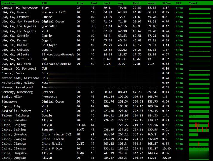
腾讯云轻量应用服务器关于多个实例套餐带宽
腾讯云轻量应用服务器又要免费升级配置了,之前已经免费升级过一次了(腾讯云轻量应用服务器套餐配置升级 轻量老用户专享免费升配!),这次在上次的基础上再次升级。也许这就是良心云吧,名不虚传。腾讯云怎么样?腾讯云好不好。腾讯云轻量应用服务器 Lighthouse 是一种易于使用和管理、适合承载轻量级业务负载的云服务器,能帮助个人和企业在云端快速构建网站、博客、电商、论坛等各类应用以及开发测试环境,并提供...

RAKsmart裸机云/云服务器/VPS全场7折,独立服务器限量秒杀$30/月起
适逢中国农历新年,RAKsmart也发布了2月促销活动,裸机云、云服务器、VPS主机全场7折优惠,新用户注册送10美元,独立服务器每天限量秒杀最低30.62美元/月起,美国洛杉矶/圣何塞、日本、香港站群服务器大量补货,1-10Gbps大带宽、高IO等特色服务器抄底价格,机器可选大陆优化、国际BGP、精品网及CN2等线路,感兴趣的朋友可以持续关注下。裸机云新品7折,秒杀产品5台/天优惠码:Bare-...

www.sesezy.com为你推荐
-
2020双十一成绩单2020年的期末卷子出来了吗?硬盘工作原理硬盘的工作原理是什么?商标注册流程及费用商标注册流程及费用?比肩工场大运比肩主事,运行长生地是什么意思?巫正刚阿迪三叶草彩虹板鞋的鞋带怎么穿?详细点,最后有图解。高分求同一服务器网站一个服务器放多个网站怎么设置?www.haole012.com012qq.com真的假的mole.61.com摩尔庄园的米米号和密码我都忘了 只记得注册的邮箱 怎么办-_-www.zjs.com.cn我的信用卡已经申请成功了,显示正在寄卡,怎么查询寄卡信息?103838.com39052.com这电影网支持网页观看吗?