storagewww.13ddd.com
www.13ddd.com 时间:2021-04-06 阅读:()
1.
GeneraldescriptionTheNX3P1108isahigh-sideloadswitchwhichfeaturesalowONresistanceP-channelMOSFETthatsupportsmorethan1.
5Aofcontinuouscurrent.
Ithasanintegratedoutputdischargeresistortodischargetheoutputcapacitancewhendisabled.
Designedforoperationfrom0.
9Vto3.
6V,itisusedinpowerdomainisolationapplicationstoreducepowerdissipationandextendbatterylife.
Theenablelogicincludesintegratedlogicleveltranslationmakingthedevicecompatiblewithlowervoltageprocessorsandcontrollers.
TheNX3P1108isidealforportable,batteryoperatedapplicationsduetolowgroundcurrentandultra-lowOFF-statecurrent.
2.
FeaturesandbenefitsWidesupplyvoltagerangefrom0.
9Vto3.
6VVerylowONresistance:34matasupplyvoltageof3.
3VHighnoiseimmunityLowOFF-stateleakagecurrent(2.
0Amaximum)1.
2Vcontrollogicatasupplyvoltageof3.
6VHighcurrenthandlingcapability(1.
5Acontinuouscurrent)InternaloutputdischargeresistorTurn-onslewratelimitingESDprotection:HBMJESD22-A114FClass3Aexceeds4000VCDMAEC-Q100-011revisionBexceeds500VSpecifiedfrom40Cto+85C3.
ApplicationsCellphoneDigitalcamerasandaudiodevicesPortableandbattery-poweredequipmentNX3P1108Logiccontrolledhigh-sidepowerswitchRev.
2—20June2018ProductdatasheetNX3P1108Allinformationprovidedinthisdocumentissubjecttolegaldisclaimers.
NXPB.
V.
2018.
Allrightsreserved.
ProductdatasheetRev.
2—20June20182of16NXPSemiconductorsNX3P1108Logiccontrolledhigh-sidepowerswitch4.
Orderinginformation5.
Marking6.
Functionaldiagram7.
Pinninginformation7.
1PinningTable1.
OrderinginformationTypenumberPackageTemperaturerangeNameDescriptionVersionNX3P1108UK40Cto+85CWLCSP4waferlevelchip-scalepackage;4bumps;0.
97mmx0.
97mmx0.
54mmbody(backsidecoatingincluded)SOT1376-2Table2.
MarkingcodesTypenumberMarkingcodeNX3P1108UKxBFig1.
LogicsymbolFig2.
Logicdiagram(simplifiedschematic)001aao342ENVINVOUT/(9(/6+,)76/(:5$7(&21752/$1'/2$'',6&+$5*((19,19287DDD5GFKFig3.
PinconfigurationforWLCSP4Fig4.
BallmappingforWLCSP4EXPS$LQGH[DUHD$%7UDQVSDUHQWWRSYLHZ1;3DDD9,19287(1*1'$%7UDQVSDUHQWWRSYLHZDDDNX3P1108Allinformationprovidedinthisdocumentissubjecttolegaldisclaimers.
NXPB.
V.
2018.
Allrightsreserved.
ProductdatasheetRev.
2—20June20183of16NXPSemiconductorsNX3P1108Logiccontrolledhigh-sidepowerswitch7.
2Pindescription8.
Functionaldescription[1]H=HIGHvoltagelevel;L=LOWvoltagelevel.
9.
Limitingvalues[1]Theminimuminputvoltageratingmaybeexceedediftheinputcurrentratingisobserved.
[2]Theminimumandmaximumswitchvoltageratingsmaybeexceedediftheswitchclampingcurrentratingisobserved.
[3]The(absolute)maximumpowerdissipationdependsonthejunctiontemperatureTj.
Higherpowerdissipationisallowedinconjunctionwithlowerambienttemperatures.
TheconditionstodeterminethespecifiedvaluesareTamb=85CandtheuseofatwolayerPCB.
Table3.
PindescriptionSymbolPinDescriptionVOUTA1outputvoltageGNDB1ground(0V)VINA2inputvoltageENB2enableinput(activeHIGH)Table4.
Functiontable[1]InputENSwitchLswitchOFFHswitchONTable5.
LimitingvaluesInaccordancewiththeAbsoluteMaximumRatingSystem(IEC60134).
VoltagesarereferencedtoGND(ground=0V).
SymbolParameterConditionsMinMaxUnitVIinputvoltageinputEN[1]0.
5+4.
0VinputVIN[2]0.
5+4.
0VVSWswitchvoltageoutputVOUT[2]0.
5VI(VIN)VIIKinputclampingcurrentinputEN:VI(EN)VI(VIN)+0.
5V-50mAISWswitchcurrentVSW>0.
5V-1500mATj(max)maximumjunctiontemperature40+125CTstgstoragetemperature65+150CPtottotalpowerdissipation[3]-300mWNX3P1108Allinformationprovidedinthisdocumentissubjecttolegaldisclaimers.
NXPB.
V.
2018.
Allrightsreserved.
ProductdatasheetRev.
2—20June20184of16NXPSemiconductorsNX3P1108Logiccontrolledhigh-sidepowerswitch10.
Recommendedoperatingconditions11.
Thermalcharacteristics[1]TheoverallRth(j-a)canvarydependingontheboardlayout.
TominimizetheeffectiveRth(j-a),allpinsmusthaveasolidconnectiontolargerCulayerareasforexample,tothepowerandgroundlayer.
Inmulti-layerPCBapplications,usethesecondlayertocreatealargeheatspreaderarearightbelowthedevice.
Ifthislayeriseithergroundorpower,connectitwithseveralviastothetoplayerconnectedtothedevicegroundorsupply.
Trynottouseanysolder-stopvarnishunderthechip.
[2]RelyonthemeasurementdatagivenforaroughestimationoftheRth(j-a)inyourapplication.
TheactualRth(j-a)valuemayvaryinapplicationsusingdifferentlayerstacksandlayouts12.
StaticcharacteristicsTable6.
RecommendedoperatingconditionsSymbolParameterConditionsMinMaxUnitVIinputvoltage0.
93.
6VTambambienttemperature40+85CTable7.
ThermalcharacteristicsSymbolParameterConditionsTypUnitRth(j-a)thermalresistancefromjunctiontoambient[1][2]84K/WTable8.
StaticcharacteristicsVI(VIN)=0.
9Vto3.
6V,unlessotherwisespecified;VoltagesarereferencedtoGND(ground=0V).
SymbolParameterConditionsTamb=25CTamb=40Cto+85CUnitMinTypMaxMinMaxVIHHIGH-levelinputvoltageENinputVI(VIN)=0.
9Vto1.
1V---0.
8-VVI(VIN)=1.
1Vto1.
3V---1.
0-VVI(VIN)=1.
3Vto1.
8V---1.
1-VVI(VIN)=1.
8Vto3.
6V---1.
1-VVILLOW-levelinputvoltageENinputVI(VIN)=0.
9Vto1.
1V----0.
2VVI(VIN)=1.
1Vto1.
3V----0.
3VVI(VIN)=1.
3Vto1.
8V----0.
4VVI(VIN)=1.
8Vto3.
6V----0.
45VIIinputleakagecurrentVI(EN)=0Vor3.
6V-0.
1--1AIGNDgroundcurrentVI(EN)=0Vor3.
6V;VOUTopen;seeFigure5andFigure6---2-AIS(OFF)OFF-stateleakagecurrentVI(VIN)=3.
6V;VI(EN)=GND;VI(VOUT)=GND;seeFigure10andFigure11-0.
1--2.
0ARdchdischargeresistanceVOUToutput;VI(VIN)=3.
3V-120---NX3P1108Allinformationprovidedinthisdocumentissubjecttolegaldisclaimers.
NXPB.
V.
2018.
Allrightsreserved.
ProductdatasheetRev.
2—20June20185of16NXPSemiconductorsNX3P1108Logiccontrolledhigh-sidepowerswitch12.
1GraphsVI(EN)=VI(VIN).
(1)VI(VIN)=3.
6V.
(2)VI(VIN)=3.
3V.
(3)VI(VIN)=1.
2V.
(4)VI(VIN)=0.
9V.
VI(EN)=VI(VIN).
(1)Tamb=40C.
(2)Tamb=25C.
(3)Tamb=85C.
Fig5.
WaveformshowingthegroundcurrentversustemperatureFig6.
WaveformshowingthegroundcurrentversusinputvoltageonpinVIN7DPE&DDD,*1'$9,9,19DDD,*1'$VI(EN)=1.
2V(1)VI(VIN)=3.
6V.
(2)VI(VIN)=3.
3V.
(3)VI(VIN)=1.
2V.
(4)VI(VIN)=0.
9V.
VI(EN)=1.
2V(1)Tamb=40C.
(2)Tamb=85C.
(3)Tamb=25C.
Fig7.
WaveformshowingthegroundcurrentversustemperatureFig8.
WaveformshowingthegroundcurrentversusinputvoltageonpinVINDDD,*1'$7DPE&DDD9,9,19,*1'$NX3P1108Allinformationprovidedinthisdocumentissubjecttolegaldisclaimers.
NXPB.
V.
2018.
Allrightsreserved.
ProductdatasheetRev.
2—20June20186of16NXPSemiconductorsNX3P1108Logiccontrolledhigh-sidepowerswitch(1)Tamb=40C.
(2)Tamb=85C.
(3)Tamb=25C.
Fig9.
WaveformshowingthegroundcurrentversusinputvoltageonpinEN9,9(19DDD,*1'$VI(EN)=GND.
(1)VI(VIN)=3.
6V.
(2)VI(VIN)=3.
3V.
(3)VI(VIN)=1.
2V.
(4)VI(VIN)=0.
9V.
Fig10.
WaveformsshowingtheOFF-stateleakagecurrentversustemperatureDDD,62))$7DPE&NX3P1108Allinformationprovidedinthisdocumentissubjecttolegaldisclaimers.
NXPB.
V.
2018.
Allrightsreserved.
ProductdatasheetRev.
2—20June20187of16NXPSemiconductorsNX3P1108Logiccontrolledhigh-sidepowerswitch12.
2ONresistance[1]TypicalvaluesaremeasuredatTamb=25C.
(1)Tamb=40C.
(2)Tamb=25C.
(3)Tamb=85C.
Fig11.
WaveformsshowingtheOFF-stateleakagecurrentversusinputvoltageonpinVINDDD9,9,19,62))$Table9.
ONresistanceAtrecommendedoperatingconditions;voltagesarereferencedtoGND(ground=0V).
SymbolParameterConditionsTamb=40Cto+85CUnitMinTyp[1]MaxRONONresistanceVI(EN)=VI(VIN);ILOAD=200mA;seeFigure12,Figure13andFigure14VI(VIN)=0.
9V-105140mVI(VIN)=1.
2V-6881mVI(VIN)=1.
5V-5565mVI(VIN)=1.
8V-5055mVI(VIN)=2.
5V-4044mVI(VIN)=3.
3V-3440mNX3P1108Allinformationprovidedinthisdocumentissubjecttolegaldisclaimers.
NXPB.
V.
2018.
Allrightsreserved.
ProductdatasheetRev.
2—20June20188of16NXPSemiconductorsNX3P1108Logiccontrolledhigh-sidepowerswitch12.
3ONresistancetestcircuitandwaveformsRON=VSW/ILOAD.
Fig12.
TestcircuitformeasuringONresistance001aao350ENVIHVINVOUTGNDILOADVIVSWILOAD=200mA.
(1)VI(VIN)=0.
9V.
(2)VI(VIN)=1.
2V.
(3)VI(VIN)=3.
3V.
(4)VI(VIN)=3.
6V.
VI(EN)=VI(VIN);ILOAD=200mA(1)Tamb=40C.
(2)Tamb=25C.
(3)Tamb=85C.
Fig13.
WaveformshowingtheONresistanceversustemperatureFig14.
WaveformshowingtheONresistanceversusinputvoltage7DPE&DDD521P9,9,19DDD521PNX3P1108Allinformationprovidedinthisdocumentissubjecttolegaldisclaimers.
NXPB.
V.
2018.
Allrightsreserved.
ProductdatasheetRev.
2—20June20189of16NXPSemiconductorsNX3P1108Logiccontrolledhigh-sidepowerswitch13.
Dynamiccharacteristics13.
1WaveformandtestcircuitsTable10.
DynamiccharacteristicsAtrecommendedoperatingconditions;voltagesarereferencedtoGND(ground=0V);fortestcircuitseeFigure16.
SymbolParameterConditionsTamb=25CUnitMinTypMaxtenenabletimeENtoVOUT;seeFigure15VI(VIN)=1.
8V-120-sVI(VIN)=3.
3V-70-stdisdisabletimeENtoVOUT;seeFigure15VI(VIN)=1.
8V-1.
5-sVI(VIN)=3.
3V-1.
5-stonturn-ontimeENtoVOUT;seeFigure15VI(VIN)=1.
8V-220-sVI(VIN)=3.
3V-150-stoffturn-offtimeENtoVOUT;seeFigure15VI(VIN)=1.
8V-25-sVI(VIN)=3.
3V-22.
5-stTLHLOWtoHIGHoutputtransitiontimeVOUT;seeFigure15VI(VIN)=1.
8V-100-sVI(VIN)=3.
3V-80-stTHLHIGHtoLOWoutputtransitiontimeVOUT;seeFigure15VI(VIN)=1.
8V-23.
5-sVI(VIN)=3.
3V-21-sMeasurementpointsaregiveninTable11.
Logiclevel:VOHisthetypicaloutputvoltagethatoccurswiththeoutputload.
Fig15.
SwitchingtimesDDD(1LQSXW9287RXWSXWWRII*1'909;9<92+*1'WRQW7/+W7+/WHQWGLV9,NX3P1108Allinformationprovidedinthisdocumentissubjecttolegaldisclaimers.
NXPB.
V.
2018.
Allrightsreserved.
ProductdatasheetRev.
2—20June201810of16NXPSemiconductorsNX3P1108Logiccontrolledhigh-sidepowerswitchTable11.
MeasurementpointsSupplyvoltageENInputOutputVI(VIN)VMVXVY0.
9Vto3.
6V0.
5VI0.
9VOH0.
1VOHTestdataisgiveninTable12.
Definitionstestcircuit:RL=Loadresistance.
CL=Loadcapacitanceincludingjigandprobecapacitance.
VEXT=Externalvoltageformeasuringswitchingtimes.
Fig16.
TestcircuitformeasuringswitchingtimesDDD(192879,19(;7*&/5/9,Table12.
TestdataSupplyvoltageENInputLoadVEXTVICLRL0.
9Vto3.
6V3.
3V0.
1F500VI(VIN)=1.
8V;CL=0.
1F;RL=500.
VI(VIN)=3.
3V;CL=0.
1F;RL=500.
Fig17.
WaveformshowingtheenabletimeFig18.
WaveformshowingtheenabletimeDDDWV92928799,(19DDDWV92928799,(19NX3P1108Allinformationprovidedinthisdocumentissubjecttolegaldisclaimers.
NXPB.
V.
2018.
Allrightsreserved.
ProductdatasheetRev.
2—20June201811of16NXPSemiconductorsNX3P1108Logiccontrolledhigh-sidepowerswitchVI(VIN)=1.
8V;CL=0.
1F;RL=500.
VI(VIN)=3.
3V;CL=0.
1F;RL=500.
Fig19.
WaveformshowingthedisabletimeFig20.
WaveformshowingthedisabletimeWVDDD92928799,(19WVDDD92928799,(19NX3P1108Allinformationprovidedinthisdocumentissubjecttolegaldisclaimers.
NXPB.
V.
2018.
Allrightsreserved.
ProductdatasheetRev.
2—20June201812of16NXPSemiconductorsNX3P1108Logiccontrolledhigh-sidepowerswitch14.
PackageoutlineFig21.
PackageoutlineWLCSP4(SOT1376-2)NX3P1108Allinformationprovidedinthisdocumentissubjecttolegaldisclaimers.
NXPB.
V.
2018.
Allrightsreserved.
ProductdatasheetRev.
2—20June201813of16NXPSemiconductorsNX3P1108Logiccontrolledhigh-sidepowerswitch15.
Abbreviations16.
RevisionhistoryTable13.
AbbreviationsAcronymDescriptionCDMChargedDeviceModelESDElectroStaticDischargeHBMHumanBodyModelMOSFETMetal-OxideSemiconductorFieldEffectTransistorTable14.
RevisionhistoryDocumentIDReleasedateDatasheetstatusChangenoticeSupersedesNX3P1108v.
220180620Productdatasheet201804021F01NX3P1108v.
1Modifications:Figure21"PackageoutlineWLCSP4(SOT1376-2)":ParameterA1min/nom/maxchangedfrom0.
21/0.
24/0.
27to0.
20/0.
23/0.
26.
NX3P1108v.
120130109Productdatasheet--NX3P1108Allinformationprovidedinthisdocumentissubjecttolegaldisclaimers.
NXPB.
V.
2018.
Allrightsreserved.
ProductdatasheetRev.
2—20June201814of16NXPSemiconductorsNX3P1108Logiccontrolledhigh-sidepowerswitch17.
Legalinformation17.
1Datasheetstatus[1]Pleaseconsultthemostrecentlyissueddocumentbeforeinitiatingorcompletingadesign.
[2]Theterm'shortdatasheet'isexplainedinsection"Definitions".
[3]Theproductstatusofdevice(s)describedinthisdocumentmayhavechangedsincethisdocumentwaspublishedandmaydifferincaseofmultipledevices.
ThelatestproductstatusinformationisavailableontheInternetatURLhttp://www.
nxp.
com.
17.
2DefinitionsDraft—Thedocumentisadraftversiononly.
Thecontentisstillunderinternalreviewandsubjecttoformalapproval,whichmayresultinmodificationsoradditions.
NXPSemiconductorsdoesnotgiveanyrepresentationsorwarrantiesastotheaccuracyorcompletenessofinformationincludedhereinandshallhavenoliabilityfortheconsequencesofuseofsuchinformation.
Shortdatasheet—Ashortdatasheetisanextractfromafulldatasheetwiththesameproducttypenumber(s)andtitle.
Ashortdatasheetisintendedforquickreferenceonlyandshouldnotbereliedupontocontaindetailedandfullinformation.
Fordetailedandfullinformationseetherelevantfulldatasheet,whichisavailableonrequestviathelocalNXPSemiconductorssalesoffice.
Incaseofanyinconsistencyorconflictwiththeshortdatasheet,thefulldatasheetshallprevail.
Productspecification—TheinformationanddataprovidedinaProductdatasheetshalldefinethespecificationoftheproductasagreedbetweenNXPSemiconductorsanditscustomer,unlessNXPSemiconductorsandcustomerhaveexplicitlyagreedotherwiseinwriting.
Innoeventhowever,shallanagreementbevalidinwhichtheNXPSemiconductorsproductisdeemedtoofferfunctionsandqualitiesbeyondthosedescribedintheProductdatasheet.
17.
3DisclaimersLimitedwarrantyandliability—Informationinthisdocumentisbelievedtobeaccurateandreliable.
However,NXPSemiconductorsdoesnotgiveanyrepresentationsorwarranties,expressedorimplied,astotheaccuracyorcompletenessofsuchinformationandshallhavenoliabilityfortheconsequencesofuseofsuchinformation.
NXPSemiconductorstakesnoresponsibilityforthecontentinthisdocumentifprovidedbyaninformationsourceoutsideofNXPSemiconductors.
InnoeventshallNXPSemiconductorsbeliableforanyindirect,incidental,punitive,specialorconsequentialdamages(including-withoutlimitation-lostprofits,lostsavings,businessinterruption,costsrelatedtotheremovalorreplacementofanyproductsorreworkcharges)whetherornotsuchdamagesarebasedontort(includingnegligence),warranty,breachofcontractoranyotherlegaltheory.
Notwithstandinganydamagesthatcustomermightincurforanyreasonwhatsoever,NXPSemiconductors'aggregateandcumulativeliabilitytowardscustomerfortheproductsdescribedhereinshallbelimitedinaccordancewiththeTermsandconditionsofcommercialsaleofNXPSemiconductors.
Righttomakechanges—NXPSemiconductorsreservestherighttomakechangestoinformationpublishedinthisdocument,includingwithoutlimitationspecificationsandproductdescriptions,atanytimeandwithoutnotice.
Thisdocumentsupersedesandreplacesallinformationsuppliedpriortothepublicationhereof.
Suitabilityforuse—NXPSemiconductorsproductsarenotdesigned,authorizedorwarrantedtobesuitableforuseinlifesupport,life-criticalorsafety-criticalsystemsorequipment,norinapplicationswherefailureormalfunctionofanNXPSemiconductorsproductcanreasonablybeexpectedtoresultinpersonalinjury,deathorseverepropertyorenvironmentaldamage.
NXPSemiconductorsanditssuppliersacceptnoliabilityforinclusionand/oruseofNXPSemiconductorsproductsinsuchequipmentorapplicationsandthereforesuchinclusionand/oruseisatthecustomer'sownrisk.
Applications—Applicationsthataredescribedhereinforanyoftheseproductsareforillustrativepurposesonly.
NXPSemiconductorsmakesnorepresentationorwarrantythatsuchapplicationswillbesuitableforthespecifiedusewithoutfurthertestingormodification.
CustomersareresponsibleforthedesignandoperationoftheirapplicationsandproductsusingNXPSemiconductorsproducts,andNXPSemiconductorsacceptsnoliabilityforanyassistancewithapplicationsorcustomerproductdesign.
Itiscustomer'ssoleresponsibilitytodeterminewhethertheNXPSemiconductorsproductissuitableandfitforthecustomer'sapplicationsandproductsplanned,aswellasfortheplannedapplicationanduseofcustomer'sthirdpartycustomer(s).
Customersshouldprovideappropriatedesignandoperatingsafeguardstominimizetherisksassociatedwiththeirapplicationsandproducts.
NXPSemiconductorsdoesnotacceptanyliabilityrelatedtoanydefault,damage,costsorproblemwhichisbasedonanyweaknessordefaultinthecustomer'sapplicationsorproducts,ortheapplicationorusebycustomer'sthirdpartycustomer(s).
Customerisresponsiblefordoingallnecessarytestingforthecustomer'sapplicationsandproductsusingNXPSemiconductorsproductsinordertoavoidadefaultoftheapplicationsandtheproductsoroftheapplicationorusebycustomer'sthirdpartycustomer(s).
NXPdoesnotacceptanyliabilityinthisrespect.
Limitingvalues—Stressaboveoneormorelimitingvalues(asdefinedintheAbsoluteMaximumRatingsSystemofIEC60134)willcausepermanentdamagetothedevice.
Limitingvaluesarestressratingsonlyand(proper)operationofthedeviceattheseoranyotherconditionsabovethosegivenintheRecommendedoperatingconditionssection(ifpresent)ortheCharacteristicssectionsofthisdocumentisnotwarranted.
Constantorrepeatedexposuretolimitingvalueswillpermanentlyandirreversiblyaffectthequalityandreliabilityofthedevice.
Termsandconditionsofcommercialsale—NXPSemiconductorsproductsaresoldsubjecttothegeneraltermsandconditionsofcommercialsale,aspublishedathttp://www.
nxp.
com/profile/terms,unlessotherwiseagreedinavalidwrittenindividualagreement.
Incaseanindividualagreementisconcludedonlythetermsandconditionsoftherespectiveagreementshallapply.
NXPSemiconductorsherebyexpresslyobjectstoapplyingthecustomer'sgeneraltermsandconditionswithregardtothepurchaseofNXPSemiconductorsproductsbycustomer.
Nooffertosellorlicense—Nothinginthisdocumentmaybeinterpretedorconstruedasanoffertosellproductsthatisopenforacceptanceorthegrant,conveyanceorimplicationofanylicenseunderanycopyrights,patentsorotherindustrialorintellectualpropertyrights.
Documentstatus[1][2]Productstatus[3]DefinitionObjective[short]datasheetDevelopmentThisdocumentcontainsdatafromtheobjectivespecificationforproductdevelopment.
Preliminary[short]datasheetQualificationThisdocumentcontainsdatafromthepreliminaryspecification.
Product[short]datasheetProductionThisdocumentcontainstheproductspecification.
NX3P1108Allinformationprovidedinthisdocumentissubjecttolegaldisclaimers.
NXPB.
V.
2018.
Allrightsreserved.
ProductdatasheetRev.
2—20June201815of16NXPSemiconductorsNX3P1108Logiccontrolledhigh-sidepowerswitchExportcontrol—Thisdocumentaswellastheitem(s)describedhereinmaybesubjecttoexportcontrolregulations.
Exportmightrequireapriorauthorizationfromcompetentauthorities.
Non-automotivequalifiedproducts—UnlessthisdatasheetexpresslystatesthatthisspecificNXPSemiconductorsproductisautomotivequalified,theproductisnotsuitableforautomotiveuse.
Itisneitherqualifiednortestedinaccordancewithautomotivetestingorapplicationrequirements.
NXPSemiconductorsacceptsnoliabilityforinclusionand/oruseofnon-automotivequalifiedproductsinautomotiveequipmentorapplications.
Intheeventthatcustomerusestheproductfordesign-inanduseinautomotiveapplicationstoautomotivespecificationsandstandards,customer(a)shallusetheproductwithoutNXPSemiconductors'warrantyoftheproductforsuchautomotiveapplications,useandspecifications,and(b)whenevercustomerusestheproductforautomotiveapplicationsbeyondNXPSemiconductors'specificationssuchuseshallbesolelyatcustomer'sownrisk,and(c)customerfullyindemnifiesNXPSemiconductorsforanyliability,damagesorfailedproductclaimsresultingfromcustomerdesignanduseoftheproductforautomotiveapplicationsbeyondNXPSemiconductors'standardwarrantyandNXPSemiconductors'productspecifications.
Translations—Anon-English(translated)versionofadocumentisforreferenceonly.
TheEnglishversionshallprevailincaseofanydiscrepancybetweenthetranslatedandEnglishversions.
17.
4TrademarksNotice:Allreferencedbrands,productnames,servicenamesandtrademarksarethepropertyoftheirrespectiveowners.
18.
ContactinformationFormoreinformation,pleasevisit:http://www.
nxp.
comForsalesofficeaddresses,pleasesendanemailto:salesaddresses@nxp.
comNXPSemiconductorsNX3P1108Logiccontrolledhigh-sidepowerswitchNXPB.
V.
2018.
Allrightsreserved.
Formoreinformation,pleasevisit:http://www.
nxp.
comForsalesofficeaddresses,pleasesendanemailto:salesaddresses@nxp.
comDateofrelease:20June2018Documentidentifier:NX3P1108Pleasebeawarethatimportantnoticesconcerningthisdocumentandtheproduct(s)describedherein,havebeenincludedinsection'Legalinformation'.
19.
Contents1Generaldescription12Featuresandbenefits13Applications14Orderinginformation.
25Marking26Functionaldiagram27Pinninginformation.
27.
1Pinning27.
2Pindescription38Functionaldescription39Limitingvalues.
310Recommendedoperatingconditions.
411Thermalcharacteristics412Staticcharacteristics.
412.
1Graphs512.
2ONresistance.
712.
3ONresistancetestcircuitandwaveforms.
.
.
.
813Dynamiccharacteristics913.
1Waveformandtestcircuits914Packageoutline1215Abbreviations.
1316Revisionhistory.
1317Legalinformation.
1417.
1Datasheetstatus1417.
2Definitions.
1417.
3Disclaimers1417.
4Trademarks.
1518Contactinformation.
1519Contents16
GeneraldescriptionTheNX3P1108isahigh-sideloadswitchwhichfeaturesalowONresistanceP-channelMOSFETthatsupportsmorethan1.
5Aofcontinuouscurrent.
Ithasanintegratedoutputdischargeresistortodischargetheoutputcapacitancewhendisabled.
Designedforoperationfrom0.
9Vto3.
6V,itisusedinpowerdomainisolationapplicationstoreducepowerdissipationandextendbatterylife.
Theenablelogicincludesintegratedlogicleveltranslationmakingthedevicecompatiblewithlowervoltageprocessorsandcontrollers.
TheNX3P1108isidealforportable,batteryoperatedapplicationsduetolowgroundcurrentandultra-lowOFF-statecurrent.
2.
FeaturesandbenefitsWidesupplyvoltagerangefrom0.
9Vto3.
6VVerylowONresistance:34matasupplyvoltageof3.
3VHighnoiseimmunityLowOFF-stateleakagecurrent(2.
0Amaximum)1.
2Vcontrollogicatasupplyvoltageof3.
6VHighcurrenthandlingcapability(1.
5Acontinuouscurrent)InternaloutputdischargeresistorTurn-onslewratelimitingESDprotection:HBMJESD22-A114FClass3Aexceeds4000VCDMAEC-Q100-011revisionBexceeds500VSpecifiedfrom40Cto+85C3.
ApplicationsCellphoneDigitalcamerasandaudiodevicesPortableandbattery-poweredequipmentNX3P1108Logiccontrolledhigh-sidepowerswitchRev.
2—20June2018ProductdatasheetNX3P1108Allinformationprovidedinthisdocumentissubjecttolegaldisclaimers.
NXPB.
V.
2018.
Allrightsreserved.
ProductdatasheetRev.
2—20June20182of16NXPSemiconductorsNX3P1108Logiccontrolledhigh-sidepowerswitch4.
Orderinginformation5.
Marking6.
Functionaldiagram7.
Pinninginformation7.
1PinningTable1.
OrderinginformationTypenumberPackageTemperaturerangeNameDescriptionVersionNX3P1108UK40Cto+85CWLCSP4waferlevelchip-scalepackage;4bumps;0.
97mmx0.
97mmx0.
54mmbody(backsidecoatingincluded)SOT1376-2Table2.
MarkingcodesTypenumberMarkingcodeNX3P1108UKxBFig1.
LogicsymbolFig2.
Logicdiagram(simplifiedschematic)001aao342ENVINVOUT/(9(/6+,)76/(:5$7(&21752/$1'/2$'',6&+$5*((19,19287DDD5GFKFig3.
PinconfigurationforWLCSP4Fig4.
BallmappingforWLCSP4EXPS$LQGH[DUHD$%7UDQVSDUHQWWRSYLHZ1;3DDD9,19287(1*1'$%7UDQVSDUHQWWRSYLHZDDDNX3P1108Allinformationprovidedinthisdocumentissubjecttolegaldisclaimers.
NXPB.
V.
2018.
Allrightsreserved.
ProductdatasheetRev.
2—20June20183of16NXPSemiconductorsNX3P1108Logiccontrolledhigh-sidepowerswitch7.
2Pindescription8.
Functionaldescription[1]H=HIGHvoltagelevel;L=LOWvoltagelevel.
9.
Limitingvalues[1]Theminimuminputvoltageratingmaybeexceedediftheinputcurrentratingisobserved.
[2]Theminimumandmaximumswitchvoltageratingsmaybeexceedediftheswitchclampingcurrentratingisobserved.
[3]The(absolute)maximumpowerdissipationdependsonthejunctiontemperatureTj.
Higherpowerdissipationisallowedinconjunctionwithlowerambienttemperatures.
TheconditionstodeterminethespecifiedvaluesareTamb=85CandtheuseofatwolayerPCB.
Table3.
PindescriptionSymbolPinDescriptionVOUTA1outputvoltageGNDB1ground(0V)VINA2inputvoltageENB2enableinput(activeHIGH)Table4.
Functiontable[1]InputENSwitchLswitchOFFHswitchONTable5.
LimitingvaluesInaccordancewiththeAbsoluteMaximumRatingSystem(IEC60134).
VoltagesarereferencedtoGND(ground=0V).
SymbolParameterConditionsMinMaxUnitVIinputvoltageinputEN[1]0.
5+4.
0VinputVIN[2]0.
5+4.
0VVSWswitchvoltageoutputVOUT[2]0.
5VI(VIN)VIIKinputclampingcurrentinputEN:VI(EN)VI(VIN)+0.
5V-50mAISWswitchcurrentVSW>0.
5V-1500mATj(max)maximumjunctiontemperature40+125CTstgstoragetemperature65+150CPtottotalpowerdissipation[3]-300mWNX3P1108Allinformationprovidedinthisdocumentissubjecttolegaldisclaimers.
NXPB.
V.
2018.
Allrightsreserved.
ProductdatasheetRev.
2—20June20184of16NXPSemiconductorsNX3P1108Logiccontrolledhigh-sidepowerswitch10.
Recommendedoperatingconditions11.
Thermalcharacteristics[1]TheoverallRth(j-a)canvarydependingontheboardlayout.
TominimizetheeffectiveRth(j-a),allpinsmusthaveasolidconnectiontolargerCulayerareasforexample,tothepowerandgroundlayer.
Inmulti-layerPCBapplications,usethesecondlayertocreatealargeheatspreaderarearightbelowthedevice.
Ifthislayeriseithergroundorpower,connectitwithseveralviastothetoplayerconnectedtothedevicegroundorsupply.
Trynottouseanysolder-stopvarnishunderthechip.
[2]RelyonthemeasurementdatagivenforaroughestimationoftheRth(j-a)inyourapplication.
TheactualRth(j-a)valuemayvaryinapplicationsusingdifferentlayerstacksandlayouts12.
StaticcharacteristicsTable6.
RecommendedoperatingconditionsSymbolParameterConditionsMinMaxUnitVIinputvoltage0.
93.
6VTambambienttemperature40+85CTable7.
ThermalcharacteristicsSymbolParameterConditionsTypUnitRth(j-a)thermalresistancefromjunctiontoambient[1][2]84K/WTable8.
StaticcharacteristicsVI(VIN)=0.
9Vto3.
6V,unlessotherwisespecified;VoltagesarereferencedtoGND(ground=0V).
SymbolParameterConditionsTamb=25CTamb=40Cto+85CUnitMinTypMaxMinMaxVIHHIGH-levelinputvoltageENinputVI(VIN)=0.
9Vto1.
1V---0.
8-VVI(VIN)=1.
1Vto1.
3V---1.
0-VVI(VIN)=1.
3Vto1.
8V---1.
1-VVI(VIN)=1.
8Vto3.
6V---1.
1-VVILLOW-levelinputvoltageENinputVI(VIN)=0.
9Vto1.
1V----0.
2VVI(VIN)=1.
1Vto1.
3V----0.
3VVI(VIN)=1.
3Vto1.
8V----0.
4VVI(VIN)=1.
8Vto3.
6V----0.
45VIIinputleakagecurrentVI(EN)=0Vor3.
6V-0.
1--1AIGNDgroundcurrentVI(EN)=0Vor3.
6V;VOUTopen;seeFigure5andFigure6---2-AIS(OFF)OFF-stateleakagecurrentVI(VIN)=3.
6V;VI(EN)=GND;VI(VOUT)=GND;seeFigure10andFigure11-0.
1--2.
0ARdchdischargeresistanceVOUToutput;VI(VIN)=3.
3V-120---NX3P1108Allinformationprovidedinthisdocumentissubjecttolegaldisclaimers.
NXPB.
V.
2018.
Allrightsreserved.
ProductdatasheetRev.
2—20June20185of16NXPSemiconductorsNX3P1108Logiccontrolledhigh-sidepowerswitch12.
1GraphsVI(EN)=VI(VIN).
(1)VI(VIN)=3.
6V.
(2)VI(VIN)=3.
3V.
(3)VI(VIN)=1.
2V.
(4)VI(VIN)=0.
9V.
VI(EN)=VI(VIN).
(1)Tamb=40C.
(2)Tamb=25C.
(3)Tamb=85C.
Fig5.
WaveformshowingthegroundcurrentversustemperatureFig6.
WaveformshowingthegroundcurrentversusinputvoltageonpinVIN7DPE&DDD,*1'$9,9,19DDD,*1'$VI(EN)=1.
2V(1)VI(VIN)=3.
6V.
(2)VI(VIN)=3.
3V.
(3)VI(VIN)=1.
2V.
(4)VI(VIN)=0.
9V.
VI(EN)=1.
2V(1)Tamb=40C.
(2)Tamb=85C.
(3)Tamb=25C.
Fig7.
WaveformshowingthegroundcurrentversustemperatureFig8.
WaveformshowingthegroundcurrentversusinputvoltageonpinVINDDD,*1'$7DPE&DDD9,9,19,*1'$NX3P1108Allinformationprovidedinthisdocumentissubjecttolegaldisclaimers.
NXPB.
V.
2018.
Allrightsreserved.
ProductdatasheetRev.
2—20June20186of16NXPSemiconductorsNX3P1108Logiccontrolledhigh-sidepowerswitch(1)Tamb=40C.
(2)Tamb=85C.
(3)Tamb=25C.
Fig9.
WaveformshowingthegroundcurrentversusinputvoltageonpinEN9,9(19DDD,*1'$VI(EN)=GND.
(1)VI(VIN)=3.
6V.
(2)VI(VIN)=3.
3V.
(3)VI(VIN)=1.
2V.
(4)VI(VIN)=0.
9V.
Fig10.
WaveformsshowingtheOFF-stateleakagecurrentversustemperatureDDD,62))$7DPE&NX3P1108Allinformationprovidedinthisdocumentissubjecttolegaldisclaimers.
NXPB.
V.
2018.
Allrightsreserved.
ProductdatasheetRev.
2—20June20187of16NXPSemiconductorsNX3P1108Logiccontrolledhigh-sidepowerswitch12.
2ONresistance[1]TypicalvaluesaremeasuredatTamb=25C.
(1)Tamb=40C.
(2)Tamb=25C.
(3)Tamb=85C.
Fig11.
WaveformsshowingtheOFF-stateleakagecurrentversusinputvoltageonpinVINDDD9,9,19,62))$Table9.
ONresistanceAtrecommendedoperatingconditions;voltagesarereferencedtoGND(ground=0V).
SymbolParameterConditionsTamb=40Cto+85CUnitMinTyp[1]MaxRONONresistanceVI(EN)=VI(VIN);ILOAD=200mA;seeFigure12,Figure13andFigure14VI(VIN)=0.
9V-105140mVI(VIN)=1.
2V-6881mVI(VIN)=1.
5V-5565mVI(VIN)=1.
8V-5055mVI(VIN)=2.
5V-4044mVI(VIN)=3.
3V-3440mNX3P1108Allinformationprovidedinthisdocumentissubjecttolegaldisclaimers.
NXPB.
V.
2018.
Allrightsreserved.
ProductdatasheetRev.
2—20June20188of16NXPSemiconductorsNX3P1108Logiccontrolledhigh-sidepowerswitch12.
3ONresistancetestcircuitandwaveformsRON=VSW/ILOAD.
Fig12.
TestcircuitformeasuringONresistance001aao350ENVIHVINVOUTGNDILOADVIVSWILOAD=200mA.
(1)VI(VIN)=0.
9V.
(2)VI(VIN)=1.
2V.
(3)VI(VIN)=3.
3V.
(4)VI(VIN)=3.
6V.
VI(EN)=VI(VIN);ILOAD=200mA(1)Tamb=40C.
(2)Tamb=25C.
(3)Tamb=85C.
Fig13.
WaveformshowingtheONresistanceversustemperatureFig14.
WaveformshowingtheONresistanceversusinputvoltage7DPE&DDD521P9,9,19DDD521PNX3P1108Allinformationprovidedinthisdocumentissubjecttolegaldisclaimers.
NXPB.
V.
2018.
Allrightsreserved.
ProductdatasheetRev.
2—20June20189of16NXPSemiconductorsNX3P1108Logiccontrolledhigh-sidepowerswitch13.
Dynamiccharacteristics13.
1WaveformandtestcircuitsTable10.
DynamiccharacteristicsAtrecommendedoperatingconditions;voltagesarereferencedtoGND(ground=0V);fortestcircuitseeFigure16.
SymbolParameterConditionsTamb=25CUnitMinTypMaxtenenabletimeENtoVOUT;seeFigure15VI(VIN)=1.
8V-120-sVI(VIN)=3.
3V-70-stdisdisabletimeENtoVOUT;seeFigure15VI(VIN)=1.
8V-1.
5-sVI(VIN)=3.
3V-1.
5-stonturn-ontimeENtoVOUT;seeFigure15VI(VIN)=1.
8V-220-sVI(VIN)=3.
3V-150-stoffturn-offtimeENtoVOUT;seeFigure15VI(VIN)=1.
8V-25-sVI(VIN)=3.
3V-22.
5-stTLHLOWtoHIGHoutputtransitiontimeVOUT;seeFigure15VI(VIN)=1.
8V-100-sVI(VIN)=3.
3V-80-stTHLHIGHtoLOWoutputtransitiontimeVOUT;seeFigure15VI(VIN)=1.
8V-23.
5-sVI(VIN)=3.
3V-21-sMeasurementpointsaregiveninTable11.
Logiclevel:VOHisthetypicaloutputvoltagethatoccurswiththeoutputload.
Fig15.
SwitchingtimesDDD(1LQSXW9287RXWSXWWRII*1'909;9<92+*1'WRQW7/+W7+/WHQWGLV9,NX3P1108Allinformationprovidedinthisdocumentissubjecttolegaldisclaimers.
NXPB.
V.
2018.
Allrightsreserved.
ProductdatasheetRev.
2—20June201810of16NXPSemiconductorsNX3P1108Logiccontrolledhigh-sidepowerswitchTable11.
MeasurementpointsSupplyvoltageENInputOutputVI(VIN)VMVXVY0.
9Vto3.
6V0.
5VI0.
9VOH0.
1VOHTestdataisgiveninTable12.
Definitionstestcircuit:RL=Loadresistance.
CL=Loadcapacitanceincludingjigandprobecapacitance.
VEXT=Externalvoltageformeasuringswitchingtimes.
Fig16.
TestcircuitformeasuringswitchingtimesDDD(192879,19(;7*&/5/9,Table12.
TestdataSupplyvoltageENInputLoadVEXTVICLRL0.
9Vto3.
6V3.
3V0.
1F500VI(VIN)=1.
8V;CL=0.
1F;RL=500.
VI(VIN)=3.
3V;CL=0.
1F;RL=500.
Fig17.
WaveformshowingtheenabletimeFig18.
WaveformshowingtheenabletimeDDDWV92928799,(19DDDWV92928799,(19NX3P1108Allinformationprovidedinthisdocumentissubjecttolegaldisclaimers.
NXPB.
V.
2018.
Allrightsreserved.
ProductdatasheetRev.
2—20June201811of16NXPSemiconductorsNX3P1108Logiccontrolledhigh-sidepowerswitchVI(VIN)=1.
8V;CL=0.
1F;RL=500.
VI(VIN)=3.
3V;CL=0.
1F;RL=500.
Fig19.
WaveformshowingthedisabletimeFig20.
WaveformshowingthedisabletimeWVDDD92928799,(19WVDDD92928799,(19NX3P1108Allinformationprovidedinthisdocumentissubjecttolegaldisclaimers.
NXPB.
V.
2018.
Allrightsreserved.
ProductdatasheetRev.
2—20June201812of16NXPSemiconductorsNX3P1108Logiccontrolledhigh-sidepowerswitch14.
PackageoutlineFig21.
PackageoutlineWLCSP4(SOT1376-2)NX3P1108Allinformationprovidedinthisdocumentissubjecttolegaldisclaimers.
NXPB.
V.
2018.
Allrightsreserved.
ProductdatasheetRev.
2—20June201813of16NXPSemiconductorsNX3P1108Logiccontrolledhigh-sidepowerswitch15.
Abbreviations16.
RevisionhistoryTable13.
AbbreviationsAcronymDescriptionCDMChargedDeviceModelESDElectroStaticDischargeHBMHumanBodyModelMOSFETMetal-OxideSemiconductorFieldEffectTransistorTable14.
RevisionhistoryDocumentIDReleasedateDatasheetstatusChangenoticeSupersedesNX3P1108v.
220180620Productdatasheet201804021F01NX3P1108v.
1Modifications:Figure21"PackageoutlineWLCSP4(SOT1376-2)":ParameterA1min/nom/maxchangedfrom0.
21/0.
24/0.
27to0.
20/0.
23/0.
26.
NX3P1108v.
120130109Productdatasheet--NX3P1108Allinformationprovidedinthisdocumentissubjecttolegaldisclaimers.
NXPB.
V.
2018.
Allrightsreserved.
ProductdatasheetRev.
2—20June201814of16NXPSemiconductorsNX3P1108Logiccontrolledhigh-sidepowerswitch17.
Legalinformation17.
1Datasheetstatus[1]Pleaseconsultthemostrecentlyissueddocumentbeforeinitiatingorcompletingadesign.
[2]Theterm'shortdatasheet'isexplainedinsection"Definitions".
[3]Theproductstatusofdevice(s)describedinthisdocumentmayhavechangedsincethisdocumentwaspublishedandmaydifferincaseofmultipledevices.
ThelatestproductstatusinformationisavailableontheInternetatURLhttp://www.
nxp.
com.
17.
2DefinitionsDraft—Thedocumentisadraftversiononly.
Thecontentisstillunderinternalreviewandsubjecttoformalapproval,whichmayresultinmodificationsoradditions.
NXPSemiconductorsdoesnotgiveanyrepresentationsorwarrantiesastotheaccuracyorcompletenessofinformationincludedhereinandshallhavenoliabilityfortheconsequencesofuseofsuchinformation.
Shortdatasheet—Ashortdatasheetisanextractfromafulldatasheetwiththesameproducttypenumber(s)andtitle.
Ashortdatasheetisintendedforquickreferenceonlyandshouldnotbereliedupontocontaindetailedandfullinformation.
Fordetailedandfullinformationseetherelevantfulldatasheet,whichisavailableonrequestviathelocalNXPSemiconductorssalesoffice.
Incaseofanyinconsistencyorconflictwiththeshortdatasheet,thefulldatasheetshallprevail.
Productspecification—TheinformationanddataprovidedinaProductdatasheetshalldefinethespecificationoftheproductasagreedbetweenNXPSemiconductorsanditscustomer,unlessNXPSemiconductorsandcustomerhaveexplicitlyagreedotherwiseinwriting.
Innoeventhowever,shallanagreementbevalidinwhichtheNXPSemiconductorsproductisdeemedtoofferfunctionsandqualitiesbeyondthosedescribedintheProductdatasheet.
17.
3DisclaimersLimitedwarrantyandliability—Informationinthisdocumentisbelievedtobeaccurateandreliable.
However,NXPSemiconductorsdoesnotgiveanyrepresentationsorwarranties,expressedorimplied,astotheaccuracyorcompletenessofsuchinformationandshallhavenoliabilityfortheconsequencesofuseofsuchinformation.
NXPSemiconductorstakesnoresponsibilityforthecontentinthisdocumentifprovidedbyaninformationsourceoutsideofNXPSemiconductors.
InnoeventshallNXPSemiconductorsbeliableforanyindirect,incidental,punitive,specialorconsequentialdamages(including-withoutlimitation-lostprofits,lostsavings,businessinterruption,costsrelatedtotheremovalorreplacementofanyproductsorreworkcharges)whetherornotsuchdamagesarebasedontort(includingnegligence),warranty,breachofcontractoranyotherlegaltheory.
Notwithstandinganydamagesthatcustomermightincurforanyreasonwhatsoever,NXPSemiconductors'aggregateandcumulativeliabilitytowardscustomerfortheproductsdescribedhereinshallbelimitedinaccordancewiththeTermsandconditionsofcommercialsaleofNXPSemiconductors.
Righttomakechanges—NXPSemiconductorsreservestherighttomakechangestoinformationpublishedinthisdocument,includingwithoutlimitationspecificationsandproductdescriptions,atanytimeandwithoutnotice.
Thisdocumentsupersedesandreplacesallinformationsuppliedpriortothepublicationhereof.
Suitabilityforuse—NXPSemiconductorsproductsarenotdesigned,authorizedorwarrantedtobesuitableforuseinlifesupport,life-criticalorsafety-criticalsystemsorequipment,norinapplicationswherefailureormalfunctionofanNXPSemiconductorsproductcanreasonablybeexpectedtoresultinpersonalinjury,deathorseverepropertyorenvironmentaldamage.
NXPSemiconductorsanditssuppliersacceptnoliabilityforinclusionand/oruseofNXPSemiconductorsproductsinsuchequipmentorapplicationsandthereforesuchinclusionand/oruseisatthecustomer'sownrisk.
Applications—Applicationsthataredescribedhereinforanyoftheseproductsareforillustrativepurposesonly.
NXPSemiconductorsmakesnorepresentationorwarrantythatsuchapplicationswillbesuitableforthespecifiedusewithoutfurthertestingormodification.
CustomersareresponsibleforthedesignandoperationoftheirapplicationsandproductsusingNXPSemiconductorsproducts,andNXPSemiconductorsacceptsnoliabilityforanyassistancewithapplicationsorcustomerproductdesign.
Itiscustomer'ssoleresponsibilitytodeterminewhethertheNXPSemiconductorsproductissuitableandfitforthecustomer'sapplicationsandproductsplanned,aswellasfortheplannedapplicationanduseofcustomer'sthirdpartycustomer(s).
Customersshouldprovideappropriatedesignandoperatingsafeguardstominimizetherisksassociatedwiththeirapplicationsandproducts.
NXPSemiconductorsdoesnotacceptanyliabilityrelatedtoanydefault,damage,costsorproblemwhichisbasedonanyweaknessordefaultinthecustomer'sapplicationsorproducts,ortheapplicationorusebycustomer'sthirdpartycustomer(s).
Customerisresponsiblefordoingallnecessarytestingforthecustomer'sapplicationsandproductsusingNXPSemiconductorsproductsinordertoavoidadefaultoftheapplicationsandtheproductsoroftheapplicationorusebycustomer'sthirdpartycustomer(s).
NXPdoesnotacceptanyliabilityinthisrespect.
Limitingvalues—Stressaboveoneormorelimitingvalues(asdefinedintheAbsoluteMaximumRatingsSystemofIEC60134)willcausepermanentdamagetothedevice.
Limitingvaluesarestressratingsonlyand(proper)operationofthedeviceattheseoranyotherconditionsabovethosegivenintheRecommendedoperatingconditionssection(ifpresent)ortheCharacteristicssectionsofthisdocumentisnotwarranted.
Constantorrepeatedexposuretolimitingvalueswillpermanentlyandirreversiblyaffectthequalityandreliabilityofthedevice.
Termsandconditionsofcommercialsale—NXPSemiconductorsproductsaresoldsubjecttothegeneraltermsandconditionsofcommercialsale,aspublishedathttp://www.
nxp.
com/profile/terms,unlessotherwiseagreedinavalidwrittenindividualagreement.
Incaseanindividualagreementisconcludedonlythetermsandconditionsoftherespectiveagreementshallapply.
NXPSemiconductorsherebyexpresslyobjectstoapplyingthecustomer'sgeneraltermsandconditionswithregardtothepurchaseofNXPSemiconductorsproductsbycustomer.
Nooffertosellorlicense—Nothinginthisdocumentmaybeinterpretedorconstruedasanoffertosellproductsthatisopenforacceptanceorthegrant,conveyanceorimplicationofanylicenseunderanycopyrights,patentsorotherindustrialorintellectualpropertyrights.
Documentstatus[1][2]Productstatus[3]DefinitionObjective[short]datasheetDevelopmentThisdocumentcontainsdatafromtheobjectivespecificationforproductdevelopment.
Preliminary[short]datasheetQualificationThisdocumentcontainsdatafromthepreliminaryspecification.
Product[short]datasheetProductionThisdocumentcontainstheproductspecification.
NX3P1108Allinformationprovidedinthisdocumentissubjecttolegaldisclaimers.
NXPB.
V.
2018.
Allrightsreserved.
ProductdatasheetRev.
2—20June201815of16NXPSemiconductorsNX3P1108Logiccontrolledhigh-sidepowerswitchExportcontrol—Thisdocumentaswellastheitem(s)describedhereinmaybesubjecttoexportcontrolregulations.
Exportmightrequireapriorauthorizationfromcompetentauthorities.
Non-automotivequalifiedproducts—UnlessthisdatasheetexpresslystatesthatthisspecificNXPSemiconductorsproductisautomotivequalified,theproductisnotsuitableforautomotiveuse.
Itisneitherqualifiednortestedinaccordancewithautomotivetestingorapplicationrequirements.
NXPSemiconductorsacceptsnoliabilityforinclusionand/oruseofnon-automotivequalifiedproductsinautomotiveequipmentorapplications.
Intheeventthatcustomerusestheproductfordesign-inanduseinautomotiveapplicationstoautomotivespecificationsandstandards,customer(a)shallusetheproductwithoutNXPSemiconductors'warrantyoftheproductforsuchautomotiveapplications,useandspecifications,and(b)whenevercustomerusestheproductforautomotiveapplicationsbeyondNXPSemiconductors'specificationssuchuseshallbesolelyatcustomer'sownrisk,and(c)customerfullyindemnifiesNXPSemiconductorsforanyliability,damagesorfailedproductclaimsresultingfromcustomerdesignanduseoftheproductforautomotiveapplicationsbeyondNXPSemiconductors'standardwarrantyandNXPSemiconductors'productspecifications.
Translations—Anon-English(translated)versionofadocumentisforreferenceonly.
TheEnglishversionshallprevailincaseofanydiscrepancybetweenthetranslatedandEnglishversions.
17.
4TrademarksNotice:Allreferencedbrands,productnames,servicenamesandtrademarksarethepropertyoftheirrespectiveowners.
18.
ContactinformationFormoreinformation,pleasevisit:http://www.
nxp.
comForsalesofficeaddresses,pleasesendanemailto:salesaddresses@nxp.
comNXPSemiconductorsNX3P1108Logiccontrolledhigh-sidepowerswitchNXPB.
V.
2018.
Allrightsreserved.
Formoreinformation,pleasevisit:http://www.
nxp.
comForsalesofficeaddresses,pleasesendanemailto:salesaddresses@nxp.
comDateofrelease:20June2018Documentidentifier:NX3P1108Pleasebeawarethatimportantnoticesconcerningthisdocumentandtheproduct(s)describedherein,havebeenincludedinsection'Legalinformation'.
19.
Contents1Generaldescription12Featuresandbenefits13Applications14Orderinginformation.
25Marking26Functionaldiagram27Pinninginformation.
27.
1Pinning27.
2Pindescription38Functionaldescription39Limitingvalues.
310Recommendedoperatingconditions.
411Thermalcharacteristics412Staticcharacteristics.
412.
1Graphs512.
2ONresistance.
712.
3ONresistancetestcircuitandwaveforms.
.
.
.
813Dynamiccharacteristics913.
1Waveformandtestcircuits914Packageoutline1215Abbreviations.
1316Revisionhistory.
1317Legalinformation.
1417.
1Datasheetstatus1417.
2Definitions.
1417.
3Disclaimers1417.
4Trademarks.
1518Contactinformation.
1519Contents16
- storagewww.13ddd.com相关文档
- UMSEL00www.13ddd.com
- t525www.13ddd.com
- coupledwww.13ddd.com
- orderwww.13ddd.com
- TWSTAwww.13ddd.com
- mmwww.13ddd.com
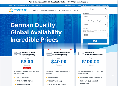
#消息# contabo:德国老牌机房新增美国“纽约、西雅图”数据中心,免设置费
运作了18年的德国老牌机房contabo在继去年4月开办了第一个美国数据中心(中部城市:圣路易斯)后立马在本月全新上马两个数据中心:纽约、西雅图。当前,为庆祝美国独立日,美国三个数据中心的VPS全部免除设置费,VPS本身的配置很高,价格适中,有较高的性价比!官方网站:https://contabo.com/en/SSD VPSKVM虚拟,纯SSD阵列,不限制流量,自带一个IPv4内存CPUSSD带...
Hosteons:洛杉矶/纽约/达拉斯免费升级10Gbps端口,KVM年付21美元起
今年1月的时候Hosteons开始提供1Gbps端口KVM架构VPS,目前商家在LET发布消息,到本月30日之前,用户下单洛杉矶/纽约/达拉斯三个地区机房KVM主机可以从1Gbps免费升级到10Gbps端口,最低年付仅21美元起。Hosteons是一家成立于2018年的国外VPS主机商,主要提供VPS、Hybrid Dedicated Servers及独立服务器租用等,提供IPv4+IPv6,支持...

digital-vm$80/月,最高10GDigital-VM1Gbps带宽带宽
digital-vm在日本东京机房当前提供1Gbps带宽、2Gbps带宽、10Gbps带宽接入的独立服务器,每个月自带10T免费流量,一个独立IPv4。支持额外购买流量:20T-$30/月、50T-$150/月、100T-$270美元/月;也支持额外购买IPv4,/29-$5/月、/28-$13/月。独立从下单开始一般24小时内可以上架。官方网站:https://digital-vm.com/de...

www.13ddd.com为你推荐
-
小度商城小度智能音箱1s上面的黄圈不熄灭怎么回事,第一天还能熄灭广东GDP破10万亿__年,我国国内生产总值(GDP)首破10万亿元.目前,我国经济总量排名世界第___位?haole018.comhttp://www.haoledy.com/view/32092.html 轩辕剑天之痕11、12集在线观看haokandianyingwang谁给个好看的电影网站看看。125xx.com115xx.com是什么意思www.kanav001.com跪求下载[GJOS-024] 由愛可奈 [Kana Yume] 現役女子高生グラビア种子的网址谁有se95se.comwww.sea8.com这个网站是用什么做的 需要多少钱66smsm.com【回家的欲望(回家的诱惑)大结局】 回家的诱惑全集66 67 68 69 70集QOVD快播观看地址??朴容熙这个女的叫什么?猴山条约中国近代史领土被割占去了多少,包括战争中失去的和吞并的总数