damagencp
ncp 时间:2021-01-11 阅读:()
SemiconductorComponentsIndustries,LLC,2014September,2014Rev.
31PublicationOrderNumber:NCP45524/DNCP45524,NCP45525ecoSWITCHtAdvancedLoadManagementControlledLoadSwitchwithLowRONTheNCP4552xseriesofloadswitchesprovideacomponentandarea-reducingsolutionforefficientpowerdomainswitchingwithinrushcurrentlimitviasoftstart.
ThesedevicesaredesignedtointegratecontrolanddriverfunctionalitywithahighperformancelowonresistancepowerMOSFETinasinglepackage.
Thiscosteffectivesolutionisidealforpowermanagementandhot-swapapplicationsrequiringlowpowerconsumptioninasmallfootprint.
FeaturesAdvancedControllerwithChargePumpIntegratedN-ChannelMOSFETwithLowRONInputVoltageRange0.
5Vto13.
5VSoft-StartviaControlledSlewRateAdjustableSlewRateControl(NCP45525)PowerGoodSignal(NCP45524)ExtremelyLowStandbyCurrentLoadBleed(QuickDischarge)ThisisaPbFreeDeviceTypicalApplicationsPortableElectronicsandSystemsNotebookandTabletComputersTelecom,Networking,Medical,andIndustrialEquipmentSetTopBoxes,Servers,andGatewaysHotSwapDevicesandPeripheralPortsFigure1.
BlockDiagram(*Note:eitherPGorSRavailableforeachpart)ENBandgap&BiasesChargePumpDelayandSlewRateControlGNDBLEEDSR*ControlLogicPG*VOUTVINVCCDFN8,2x2CASE506CCMARKINGDIAGRAMhttp://onsemi.
comRONTYPVCCIMAX18.
0mW3.
3V6A3.
3V18.
8mWVIN1.
8V5.
0VPINCONFIGURATION(TopView)Seedetailedorderingandshippinginformationonpage14ofthisdatasheet.
ORDERINGINFORMATION1XX=4HforNCP45524H=4LforNCP45524L=5HforNCP45525H=5LforNCP45525LM=DateCodeG=PbFreePackageXXMGG1(Note:Microdotmaybeineitherlocation)21.
9mW3.
3V12V1PGorSRENGNDBLEED42387659:VINVOUTVOUTVCCVINNCP45524,NCP45525http://onsemi.
com2Table1.
PINDESCRIPTIONPinNameFunction1,9VINDrainofMOSFET(0.
5V–13.
5V),Pin1mustbeconnectedtoPin92ENNCP45524H&NCP45525HActivehighdigitalinputusedtoturnontheMOSFET,pinhasaninternalpulldownresistortoGNDNCP45524L&NCP45525LActivelowdigitalinputusedtoturnontheMOSFET,pinhasaninternalpullupresistortoVCC3VCCSupplyvoltagetocontroller(3.
0V5.
5V)4GNDControllerground5BLEEDLoadbleedconnection;mustbetiedtoVOUTeitherdirectlyorthrougharesistor≤100MW.
6PGNCP45524Activehigh,opendrainoutputthatindicateswhenthegateoftheMOSFETisfullycharged,externalpullupresistor≥1kWtoanexternalvoltagesourcerequired;tietoGNDifnotusedSRNCP45525Slewrateadjustment;floatifnotused7,8VOUTSourceofMOSFETconnectedtoloadTable2.
ABSOLUTEMAXIMUMRATINGSRatingSymbolValueUnitSupplyVoltageRangeVCC0.
3to6VInputVoltageRangeVIN0.
3to18VOutputVoltageRangeVOUT0.
3to18VENDigitalInputRangeVEN0.
3to(VCC+0.
3)VPGOutputVoltageRange(Note1)VPG0.
3to6VThermalResistance,JunctiontoAmbient,SteadyState(Note2)RθJA40.
0°C/WThermalResistance,JunctiontoAmbient,SteadyState(Note3)RθJA72.
7°C/WThermalResistance,JunctiontoCase(VINPaddle)RθJC5.
3°C/WContinuousMOSFETCurrent@TA=25°CIMAX6.
0ATotalPowerDissipation@TA=25°C(Notes2and4)DerateaboveTA=25°CPD2.
5024.
9WmW/°CTotalPowerDissipation@TA=25°C(Notes3and4)DerateaboveTA=25°CPD1.
3713.
8WmW/°CStorageTemperatureRangeTSTG40to150°CLeadTemperature,Soldering(10sec.
)TSLD260°CESDCapability,HumanBodyModel(Notes5and6)ESDHBM3.
0kVESDCapability,MachineModel(Note5)ESDMM200VESDCapability,ChargedDeviceModel(Note5)ESDCDM1.
0kVLatchupCurrentImmunity(Notes5and6)LU100mAStressesexceedingthoselistedintheMaximumRatingstablemaydamagethedevice.
Ifanyoftheselimitsareexceeded,devicefunctionalityshouldnotbeassumed,damagemayoccurandreliabilitymaybeaffected.
1.
NCP45524only.
PGisanopendrainoutputthatrequiresanexternalpullupresistor≥1kWtoanexternalvoltagesource.
2.
SurfacemountedonFR4boardusing1sqinpad,1ozCu.
3.
SurfacemountedonFR4boardusingtheminimumrecommendedpadsize,1ozCu.
4.
Specifiedforderatingpurposesonly,ensurethatIMAXisneverexceeded.
5.
Testedbythefollowingmethods@TA=25°C:ESDHumanBodyModeltestedperJESD22A114ESDMachineModeltestedperJESD22A115ESDChargedDeviceModeltestedperJESD22C101LatchupCurrenttestedperJESD786.
RatingisforallpinsexceptforVINandVOUTwhicharetiedtotheinternalMOSFET'sDrainandSource.
TypicalMOSFETESDperformanceforVINandVOUTshouldbeexpectedandthesedevicesshouldbetreatedasESDsensitive.
NCP45524,NCP45525http://onsemi.
com3Table3.
OPERATINGRANGESRatingSymbolMinMaxUnitSupplyVoltageVCC35.
5VInputVoltageVIN0.
513.
5VGroundGND0VAmbientTemperatureTA4085°CJunctionTemperatureTJ40125°CFunctionaloperationabovethestresseslistedintheRecommendedOperatingRangesisnotimplied.
ExtendedexposuretostressesbeyondtheRecommendedOperatingRangeslimitsmayaffectdevicereliability.
Table4.
ELECTRICALCHARACTERISTICS(TJ=25°Cunlessotherwisespecified)ParameterConditions(Note7)SymbolMinTypMaxUnitMOSFETOnResistanceVCC=3.
3V;VIN=1.
8VRON18.
024.
0mWVCC=3.
3V;VIN=5V18.
825.
0VCC=3.
3V;VIN=12V21.
931.
7LeakageCurrent(Note8)VEN=0V;VIN=13.
5VILEAK0.
11mACONTROLLERSupplyStandbyCurrent(Note9)VEN=0V;VCC=3VISTBY0.
652mAVEN=0V;VCC=5.
5V3.
24.
5SupplyDynamicCurrent(Note10)VEN=VCC=3V;VIN=12VIDYN180300mAVEN=VCC=5.
5V;VIN=1.
8V475680BleedResistanceVEN=0V;VCC=3VRBLEED86115144WVEN=0V;VCC=5.
5V7297121ENInputHighVoltageVCC=3V5.
5VVIH2VENInputLowVoltageVCC=3V5.
5VVIL0.
8VENInputLeakageCurrentNCP45524H;NCP45525H;VEN=0VIIL90500nANCP45524L;NCP45525L;VEN=5.
5VIIH90500ENPullDownResistanceNCP45524H;NCP45525HRPD76100124kWENPullUpResistanceNCP45524L;NCP45525LRPU76100124kWPGOutputLowVoltage(Note11)NCP45524;VCC=3V;ISINK=5mAVOL0.
2VPGOutputLeakageCurrent(Note12)NCP45524;VCC=3V;VTERM=3.
3VIOH5100nASlewRateControlConstant(Note13)NCP45525;VCC=3VKSR243138mAProductparametricperformanceisindicatedintheElectricalCharacteristicsforthelistedtestconditions,unlessotherwisenoted.
ProductperformancemaynotbeindicatedbytheElectricalCharacteristicsifoperatedunderdifferentconditions.
7.
VENshownonlyforNCP45524H,NCP45525H(ENActiveHigh)unlessotherwisespecified.
8.
AveragecurrentfromVINtoVOUTwithMOSFETturnedoff.
9.
AveragecurrentfromVCCtoGNDwithMOSFETturnedoff.
10.
AveragecurrentfromVCCtoGNDafterchargeuptimeofMOSFET.
11.
PGisanopen-drainoutputthatispulledlowwhentheMOSFETisdisabled.
12.
PGisanopen-drainoutputthatisnotdrivenwhenthegateoftheMOSFETisfullycharged,requiresanexternalpullupresistor≥1kWtoanexternalvoltagesource,VTERM.
13.
SeeApplicationsInformationsectionfordetailsonhowtoadjusttheslewrate.
NCP45524,NCP45525http://onsemi.
com4Table5.
SWITCHINGCHARACTERISTICS(TJ=25°Cunlessotherwisespecified)(Notes14and15)ParameterConditionsSymbolMinTypMaxUnitOutputSlewRate(Note16)VCC=3.
3V;VIN=1.
8VSR11.
9kV/sVCC=5.
0V;VIN=1.
8V12.
1VCC=3.
3V;VIN=12V13.
5VCC=5.
0V;VIN=12V13.
9OutputTurnonDelay(Note16)VCC=3.
3V;VIN=1.
8VTON220msVCC=5.
0V;VIN=1.
8V185VCC=3.
3V;VIN=12V270VCC=5.
0V;VIN=12V260OutputTurnoffDelay(Note16)VCC=3.
3V;VIN=1.
8VTOFF1.
2msVCC=5.
0V;VIN=1.
8V0.
9VCC=3.
3V;VIN=12V0.
4VCC=5.
0V;VIN=12V0.
2PowerGoodTurnonTime(Note17)VCC=3.
3V;VIN=1.
8VTPG,ON0.
91msVCC=5.
0V;VIN=1.
8V0.
93VCC=3.
3V;VIN=12V1.
33VCC=5.
0V;VIN=12V1.
21PowerGoodTurnoffTime(Note17)VCC=3.
3V;VIN=1.
8VTPG,OFF21nsVCC=5.
0V;VIN=1.
8V15VCC=3.
3V;VIN=12V21VCC=5.
0V;VIN=12V1514.
SeebelowfigureforTestCircuitandTimingDiagram.
15.
Testedwiththefollowingconditions:VTERM=VCC;RPG=100kW;RL=10W;CL=0.
1mF.
16.
AppliestoNCP45524andNCP45525.
17.
AppliesonlytoNCP45524.
ENNCP4552xHPGGNDBLEEDOFFONSR10%90%DVDtSR=DVDt50%50%90%50%50%Figure2.
SwitchingCharacteristicsTestCircuitandTimingDiagramVOUTVINVCCCLRLVTERMRPGTPG,OFFTOFFTPG,ONTONVOUTVPGVENNCP45524,NCP45525http://onsemi.
com5TYPICALCHARACTERISTICS(TJ=25°Cunlessotherwisespecified)Figure3.
OnResistancevs.
InputVoltageFigure4.
OnResistancevs.
TemperatureVIN,INPUTVOLTAGE(V)TJ,JUNCTIONTEMPERATURE(°C)12.
510.
58.
56.
54.
52.
50.
5171819202223241057545151545101520253035Figure5.
SupplyStandbyCurrentvs.
SupplyVoltageFigure6.
SupplyStandbyCurrentvs.
TemperatureVCC,SUPPLYVOLTAGE(V)TJ,JUNCTIONTEMPERATURE(°C)5.
55.
04.
54.
03.
53.
00.
51.
01.
52.
02.
53.
03.
5105906030150304501234567Figure7.
SupplyDynamicCurrentvs.
InputVoltageFigure8.
SupplyDynamicCurrentvs.
SupplyVoltageVIN,INPUTVOLTAGE(V)VCC,SUPPLYVOLTAGE(V)12.
510.
58.
56.
54.
52.
50.
51001502503003504505005.
55.
04.
54.
03.
53.
0100200300350400500RON,ONRESISTANCE(mW)RON,ONRESISTANCE(mW)ISTBY,SUPPLYSTANDBYCURRENT(mA)21VCC=3VVCC=5.
5VVIN=1.
8VVCC=3.
3VVIN=5.
0VVIN=12V120030306090154575120VCC=3VVCC=5.
5VISTBY,SUPPLYSTANDBYCURRENT(mA)VCC=3VVCC=5.
5V400IDYN,SUPPLYDYNAMICCURRENT(mA)VIN=12VIDYN,SUPPLYDYNAMICCURRENT(mA)250450VIN=1.
8V200150NCP45524,NCP45525http://onsemi.
com6TYPICALCHARACTERISTICS(TJ=25°Cunlessotherwisespecified)Figure9.
SupplyDynamicCurrentvs.
TemperatureFigure10.
BleedResistancevs.
SupplyVoltageTJ,JUNCTIONTEMPERATURE(°C)VCC,SUPPLYVOLTAGE(V)10575451515451004005007005.
55.
04.
54.
03.
53.
095100105110115Figure11.
BleedResistancevs.
TemperatureTJ,JUNCTIONTEMPERATURE(°C)10575451515458595105115125135145Figure12.
ENPullDown/UpResistancevs.
TemperatureTJ,JUNCTIONTEMPERATURE(°C)1057545151545859095100105110115120IDYN,SUPPLYDYNAMICCURRENT(mA)RBLEED,BLEEDRESISTANCE(W)RBLEED,BLEEDRESISTANCE(W)IPD/PU,ENPULLDOWN/UPRESISTANCE(kW)300600VCC=3.
0V,VIN=12VVCC=5.
5V,VIN=1.
8VVCC=3VVCC=5.
5V200Figure13.
PGOutputLowVoltagevs.
SupplyVoltageFigure14.
PGOutputLowVoltagevs.
TemperatureVCC,SUPPLYVOLTAGE(V)TJ,JUNCTIONTEMPERATURE(°C)5.
55.
04.
54.
03.
53.
00.
1100.
1150.
1200.
1250.
1300.
1350.
14010575451515450.
080.
100.
120.
140.
160.
180.
20VOL,PGOUTPUTLOWVOLTAGE(V)VOL,PGOUTPUTLOWVOLTAGE(V)ISINK=5mAVCC=3VVCC=5.
5VISINK=5mANCP45524,NCP45525http://onsemi.
com7TYPICALCHARACTERISTICS(TJ=25°Cunlessotherwisespecified)Figure15.
SlewRateControlConstantvs.
InputVoltageFigure16.
SlewRateControlConstantvs.
TemperatureVIN,INPUTVOLTAGE(V)TJ,JUNCTIONTEMPERATURE(°C)12.
510.
58.
56.
54.
52.
50.
52931323410575451515452829303132333435Figure17.
OutputSlewRatevs.
InputVoltageVIN,INPUTVOLTAGE(V)12.
510.
58.
56.
54.
52.
50.
589101112131415KSR,SLEWRATECONTROLCONSTANT(mA)SR,OUTPUTSLEWRATE(kV/s)3033VCC=3VVCC=5.
5VVCC=3VVCC=5.
5VKSR,SLEWRATECONTROLCONSTANT(mA)VCC=3VVCC=5.
5VFigure18.
OutputSlewRatevs.
TemperatureTJ,JUNCTIONTEMPERATURE(°C)100806040200204010.
511.
011.
512.
012.
513.
013.
514.
0SR,OUTPUTSLEWRATE(kV/s)120VCC=3.
3V,VIN=12VVCC=5V,VIN=1.
8VFigure19.
OutputTurnonDelayvs.
InputVoltageVIN,INPUTVOLTAGE(V)12.
510.
58.
56.
54.
52.
50.
5150170190210230270290310Figure20.
OutputTurnonDelayvs.
TemperatureTJ,JUNCTIONTEMPERATURE(°C)1008060402002040150175200225250275300TON,OUTPUTTURNONDELAY(ms)TON,OUTPUTTURNONDELAY(ms)250VCC=3VVCC=5.
5VVCC=3.
3V,VIN=12VVCC=5V,VIN=1.
8V120NCP45524,NCP45525http://onsemi.
com8TYPICALCHARACTERISTICS(TJ=25°Cunlessotherwisespecified)Figure21.
OutputTurnoffDelayvs.
InputVoltageVIN,INPUTVOLTAGE(V)12.
510.
58.
56.
54.
52.
50.
500.
20.
40.
81.
01.
21.
61.
8Figure22.
OutputTurnoffDelayvs.
TemperatureFigure23.
PowerGoodTurnonTimevs.
InputVoltageTJ,JUNCTIONTEMPERATURE(°C)VIN,INPUTVOLTAGE(V)10080604020020400.
20.
40.
60.
81.
01.
212.
510.
58.
56.
54.
52.
50.
50.
80.
91.
11.
21.
31.
51.
71.
8TOFF,OUTPUTTURNOFFDELAY(ms)TOFF,OUTPUTTURNOFFDELAY(ms)TPG,ON,PGTURNONTIME(ms)0.
61.
4VCC=3VVCC=5.
5VVCC=3.
3V,VIN=12VVCC=5V,VIN=1.
8V120VCC=3VVCC=5.
5V1.
01.
41.
6Figure24.
PowerGoodTurnonTimevs.
TemperatureTJ,JUNCTIONTEMPERATURE(°C)10080604020020400.
80.
91.
01.
11.
21.
31.
41.
5TPG,ON,PGTURNONTIME(ms)VCC=3.
3V,VIN=12VVCC=5V,VIN=1.
8V120Figure25.
PowerGoodTurnoffTimevs.
SupplyVoltageVCC,SUPPLYVOLTAGE(V)5.
55.
04.
54.
03.
53.
012141618202224Figure26.
PowerGoodTurnoffTimevs.
TemperatureTJ,JUNCTIONTEMPERATURE(°C)100806040200204010.
012.
515.
017.
520.
022.
525.
027.
5TPG,OFF,PGTURNOFFTIME(ns)TPG,OFF,PGTURNOFFTIME(ns)VIN=0.
5VVIN=13.
5V120VCC=3.
3V,VIN=12VVCC=5V,VIN=1.
8VNCP45524,NCP45525http://onsemi.
com9APPLICATIONSINFORMATIONEnableControlBoththeNCP45524andtheNCP45525havetwopartnumbers,NCP4552x-HandNCP4552x-L,thatonlydifferinthepolarityoftheenablecontrol.
TheNCP4552x-HdevicesallowforenablingtheMOSFETinanactive-highconfiguration.
WhentheVCCsupplypinhasanadequatevoltageappliedandtheENpinisatalogichighlevel,theMOSFETwillbeenabled.
Similarly,whentheENpinisatalogiclowlevel,theMOSFETwillbedisabled.
AninternalpulldownresistortogroundontheENpinensuresthattheMOSFETwillbedisabledwhennotbeingdriven.
TheNCP4552x-LdevicesallowforenablingtheMOSFETinanactive-lowconfiguration.
WhentheVCCsupplypinhasanadequatevoltageappliedandtheENpinisatalogiclowlevel,theMOSFETwillbeenabled.
Similarly,whentheENpinisatalogichighlevel,theMOSFETwillbedisabled.
AninternalpullupresistortoVCContheENpinensuresthattheMOSFETwillbedisabledwhennotbeingdriven.
PowerSequencingTheNCP4552xdeviceswillfunctionwithanypowersequence,buttheoutputturnondelayperformancemayvaryfromwhatisspecified.
Toachievethespecifiedperformance,therearetworecommendedpowersequences:1)VCC→VIN→VEN2)VIN→VCC→VENLoadBleed(QuickDischarge)TheNCP4552xdeviceshaveaninternalbleedresistor,RBLEED,whichisusedtobleedthechargeoffoftheloadtogroundaftertheMOSFEThasbeendisabled.
InserieswiththebleedresistorisableedswitchthatisenabledwhenevertheMOSFETisdisabled.
TheMOSFETandthebleedswitchareneverconcurrentlyactive.
IsitrequiredthattheBLEEDpinbeconnectedtoVOUTeitherdirectly(asshowninFigures28and31)orthroughanexternalresistor,REXT(asshowninFigures27and30).
REXTshouldnotexceed100MWandcanbeusedtoincreasethetotalbleedresistanceanddecreasetheloadbleedrate.
CaremustbetakentoensurethatthepowerdissipatedacrossRBLEEDiskeptatasafelevel.
ThemaximumcontinuouspowerthatcanbedissipatedacrossRBLEEDis0.
4W.
REXTcanbeusedtodecreasetheamountofpowerdissipatedacrossRBLEED.
PowerGoodTheNCP45524deviceshaveapowergoodoutput(PG)thatcanbeusedtoindicatewhenthegateoftheMOSFETisfullycharged.
ThePGpinisanactive-high,open-drainoutputthatrequiresanexternalpullupresistor,RPG,greaterthanorequalto1kWtoanexternalvoltagesource,VTERM,thatiscompatiblewithinputlevelsofalldevicesconnectedtothispin(asshowninFigures27and28).
Thepowergoodoutputcanbeusedastheenablesignalforotheractivehighdevicesinthesystem(asshowninFigure29).
Thisallowsforguaranteedbydesignpowersequencingandreducesthenumberofenablesignalsneededfromthesystemcontroller.
Ifthepowergoodfeatureisnotusedintheapplication,thePGpinshouldbetiedtoGND.
SlewRateControlTheNCP4552xdevicesareequippedwithcontrolledoutputslewratewhichprovidessoftstartfunctionality.
Thislimitstheinrushcurrentcausedbycapacitorchargingandenablesthesedevicestobeusedinhotswapapplications.
TheslewrateoftheNCP45525canbedecreasedwithanexternalcapacitoraddedbetweentheSRpinandground(asshowninFigures30and31).
Withanexternalcapacitorpresent,theslewratecanbedeterminedbythefollowingequation:SlewRate+KSRCSR[Vńs](eq.
1)whereKSRisthespecifiedslewratecontrolconstant,foundinTable4,andCSRistheslewratecontrolcapacitoraddedbetweentheSRpinandground.
Theslewrateofthedevicewillalwaysbethelowerofthedefaultslewrateandtheadjustedslewrate.
Therefore,iftheCSRisnotlargeenoughtodecreasetheslewratemorethanthespecifieddefaultvalue,theslewrateofthedevicewillbethedefaultvalue.
TheSRpincanbeleftfloatingiftheslewratedoesnotneedtobedecreased.
NCP45524,NCP45525http://onsemi.
com10Figure27.
NCP45524TypicalApplicationDiagramLoadSwitchBandgap&BiasesChargePumpDelayandSlewRateControlControlLogicLoadController3.
0V5.
5VPowerSupplyorBattery0.
5V13.
5VGNDBLEEDVOUTVINPGENVCCRPG100kWVTERM=3.
3VREXTFigure28.
NCP45524TypicalApplicationDiagramHotSwapBandgap&BiasesChargePumpDelayandSlewRateControlControlLogicLoadENPGGNDBACKPLANEREMOVABLECARDGNDBLEEDVOUTPGENVCCVINRPGVTERMVIN0.
5V13.
5VVCC3.
0V5.
5VNCP45524,NCP45525http://onsemi.
com11Figure29.
NCP45524SimplifiedApplicationDiagramPowerSequencingwithPGOutputPGNCP45524HENControllerPGNCP45524HENPGRPD100kWPGRPD100kWRPG10kWVTERM=3.
3VFigure30.
NCP45525TypicalApplicationDiagramLoadSwitchBandgap&BiasesChargePumpDelayandSlewRateControlControlLogicLoadController3.
0V5.
5VPowerSupplyorBattery0.
5V13.
5VSRGNDCSRBLEEDVOUTREXTVINVCCENNCP45524,NCP45525http://onsemi.
com12Bandgap&BiasesChargePumpDelayandSlewRateControlControlLogicLoad3.
0V5.
5VENGNDBACKPLANEREMOVABLECARDFigure31.
NCP45525TypicalApplicationDiagramHotSwapVCCENVINVCCSRGNDBLEEDCSRVOUT0.
5V13.
5VVINNCP45524,NCP45525http://onsemi.
com13PACKAGEDIMENSIONSDFN82x2,0.
5PCASE506CCISSUEONOTES:1.
DIMENSIONINGANDTOLERANCINGPERASMEY14.
5M,1994.
2.
CONTROLLINGDIMENSION:MILLIMETERS.
3.
DIMENSIONbAPPLIESTOPLATEDTERMINALANDISMEASUREDBETWEEN0.
15AND0.
30MMFROMTERMINALTIP.
4.
COPLANARITYAPPLIESTOTHEEXPOSEDPADASWELLASTHETERMINALS.
ADEBC0.
10PINONE2XREFERENCE2XTOPVIEWSIDEVIEWBOTTOMVIEWLD2E2CC0.
10C0.
10C0.
08A1SEATINGPLANE8XNOTE3b8X0.
10C0.
05CABBDIMMINMAXMILLIMETERSA0.
801.
00A10.
000.
05b0.
200.
30D2.
00BSCD21.
501.
70E2.
00BSCE20.
801.
00e0.
50BSCL0.
180.
38148*ForadditionalinformationonourPbFreestrategyandsolderingdetails,pleasedownloadtheONSemiconductorSolderingandMountingTechniquesReferenceManual,SOLDERRM/D.
SOLDERINGFOOTPRINT*0.
50PITCH1.
002.
301DIMENSIONS:MILLIMETERS0.
508XNOTE40.
308XDETAILAA30.
20REFA3ADETAILBA1A3DETAILBMOLDCMPDEXPOSEDCuL10.
15OUTLINEPACKAGEeRECOMMENDEDK0.
27REF51.
70KALTERNATECONSTRUCTIONL1DETAILALALTERNATECONSTRUCTIONSLe/20.
20NCP45524,NCP45525http://onsemi.
com14ORDERINGINFORMATIONDevicePin6FunctionalityENPolarityPackageShippingNCP45524IMNTWGHPGActiveHighDFN8(PbFree)3000/Tape&ReelNCP45524IMNTWGLPGActiveLowNCP45525IMNTWGHSRActiveHighNCP45525IMNTWGLSRActiveLowForinformationontapeandreelspecifications,includingpartorientationandtapesizes,pleaserefertoourTapeandReelPackagingSpecificationsBrochure,BRD8011/D.
ONSemiconductorandareregisteredtrademarksofSemiconductorComponentsIndustries,LLC(SCILLC).
SCILLCownstherightstoanumberofpatents,trademarks,copyrights,tradesecrets,andotherintellectualproperty.
AlistingofSCILLC'sproduct/patentcoveragemaybeaccessedatwww.
onsemi.
com/site/pdf/PatentMarking.
pdf.
SCILLCreservestherighttomakechangeswithoutfurthernoticetoanyproductsherein.
SCILLCmakesnowarranty,representationorguaranteeregardingthesuitabilityofitsproductsforanyparticularpurpose,nordoesSCILLCassumeanyliabilityarisingoutoftheapplicationoruseofanyproductorcircuit,andspecificallydisclaimsanyandallliability,includingwithoutlimitationspecial,consequentialorincidentaldamages.
"Typical"parameterswhichmaybeprovidedinSCILLCdatasheetsand/orspecificationscananddovaryindifferentapplicationsandactualperformancemayvaryovertime.
Alloperatingparameters,including"Typicals"mustbevalidatedforeachcustomerapplicationbycustomer'stechnicalexperts.
SCILLCdoesnotconveyanylicenseunderitspatentrightsnortherightsofothers.
SCILLCproductsarenotdesigned,intended,orauthorizedforuseascomponentsinsystemsintendedforsurgicalimplantintothebody,orotherapplicationsintendedtosupportorsustainlife,orforanyotherapplicationinwhichthefailureoftheSCILLCproductcouldcreateasituationwherepersonalinjuryordeathmayoccur.
ShouldBuyerpurchaseoruseSCILLCproductsforanysuchunintendedorunauthorizedapplication,BuyershallindemnifyandholdSCILLCanditsofficers,employees,subsidiaries,affiliates,anddistributorsharmlessagainstallclaims,costs,damages,andexpenses,andreasonableattorneyfeesarisingoutof,directlyorindirectly,anyclaimofpersonalinjuryordeathassociatedwithsuchunintendedorunauthorizeduse,evenifsuchclaimallegesthatSCILLCwasnegligentregardingthedesignormanufactureofthepart.
SCILLCisanEqualOpportunity/AffirmativeActionEmployer.
Thisliteratureissubjecttoallapplicablecopyrightlawsandisnotforresaleinanymanner.
PUBLICATIONORDERINGINFORMATIONN.
AmericanTechnicalSupport:8002829855TollFreeUSA/CanadaEurope,MiddleEastandAfricaTechnicalSupport:Phone:421337902910JapanCustomerFocusCenterPhone:81358171050NCP45524/DecoSWITCHisatrademarkofSemiconductorComponentsIndustries,LLC(SCILLC).
LITERATUREFULFILLMENT:LiteratureDistributionCenterforONSemiconductorP.
O.
Box5163,Denver,Colorado80217USAPhone:3036752175or8003443860TollFreeUSA/CanadaFax:3036752176or8003443867TollFreeUSA/CanadaEmail:orderlit@onsemi.
comONSemiconductorWebsite:www.
onsemi.
comOrderLiterature:http://www.
onsemi.
com/orderlitForadditionalinformation,pleasecontactyourlocalSalesRepresentative
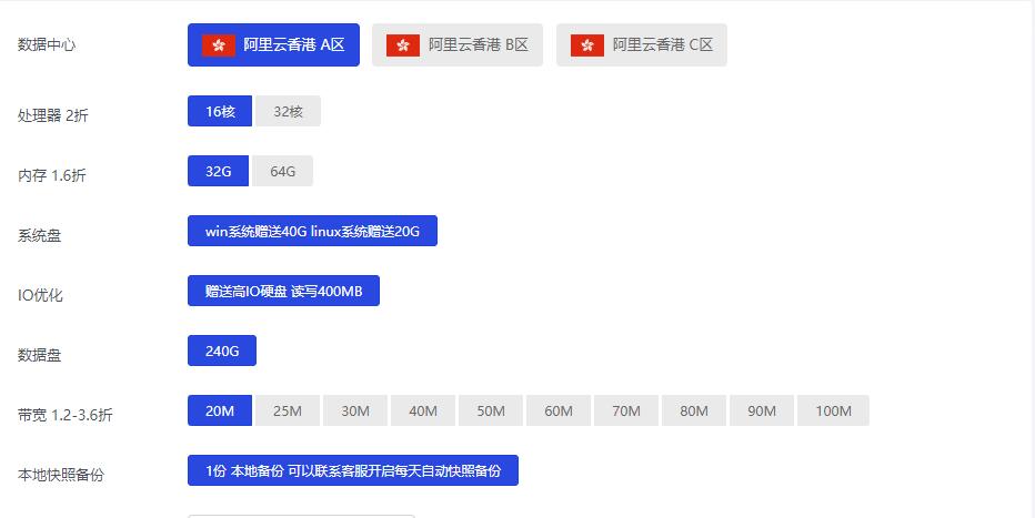
阿里云香港 16核32G 20M 999元/月
阿里云香港配置图提速啦是成立于2012年的十分老牌的一个商家这次给大家评测的是 阿里云香港 16核32G 20M 这款产品,单单说价格上就是十分的离谱原价8631元/月的现价只要 999元 而且还有个8折循环优惠。废话不多说直接进入正题。优惠时间 2021年8月20日-2021年9月20日 优惠码 wn789 8折优惠阿里云香港BGP专线 16核32G 10M带宽 优惠购买 399元购买链接阿里云...
[6.18]DogYun:充100送10元,态云7折,经典云8折,独立服务器月省100元,幸运大转盘最高5折
DogYun是一家2019年成立的国人主机商,提供VPS和独立服务器租用等,数据中心包括中国香港、美国洛杉矶、日本、韩国、德国、荷兰等,其中VPS包括常规VPS(经典云)和按小时计费VPS(动态云),使用自行开发的面板和管理系统,支持自定义配置,动态云各个硬件独立按小时计费,带宽按照用户使用量计费(不使用不计费)或者购买流量包,线路也可以自行切换。目前商家发布了6.18促销方案,新购动态云7折,经...

舍利云:海外云服务器,6核16G超大带宽vps;支持全球范围,原价516,折后价200元/月!
舍利云怎么样?舍利云推出了6核16G超大带宽316G高性能SSD和CPU,支持全球范围,原价516,折后价200元一月。原价80美元,现价30美元,支持地区:日本,新加坡,荷兰,法国,英国,澳大利亚,加拿大,韩国,美国纽约,美国硅谷,美国洛杉矶,美国亚特兰大,美国迈阿密州,美国西雅图,美国芝加哥,美国达拉斯。舍利云是vps云服务器的销售商家,其产品主要的特色是适合seo和建站,性价比方面非常不错,...

ncp为你推荐
-
买虚拟主机最近想买虚拟主机,有不限流量的虚拟主机这个怎么样靠谱吗?租服务器租服务器是什么意思?asp主机请问虚似主机和Asp服务器软件都是一个意思吗海外服务器租用国外服务器租用与国内服务器租用有哪些区别域名服务商最好的域名服务商是哪一家成都虚拟空间成都市规划信息技术中心如何?什么是虚拟主机虚拟主机是什么虚拟主机管理系统虚拟主机管理系统那一家好?天津虚拟主机在天津哪个地方能买到较好的价格又实惠还可以送货上门的虚拟主机!天津虚拟主机在天津做个网站需要多少钱