Pullabilitywww.99cycy.com
www.99cycy.com 时间:2021-03-18 阅读:()
CDCE949-Q1www.
ti.
comSCAS891–FEBRUARY2010PROGRAMMABLE4-PLLVCXOCLOCKSYNTHESIZERWITH1.
8-V,2.
5-,Vand3.
3-VLVCMOSOUTPUTSCheckforSamples:CDCE949-Q11FEATURESQualifiedforAutomotiveApplicationsSelectableOutputFrequencyupto230MHzMemberofProgrammableClockGeneratorFlexibleInputClockingConceptFamily–ExternalCrystal:8to32MHz–CDCE913/CDCEL913:1PLLs,3Outputs–On-ChipVCXO:Pull-Range±150ppm–CDCE925/CDCEL925:2PLLs,5Outputs–Single-EndedLVCMOSupto160MHz–CDCE937/CDCEL937:3PLLs,7OutputsLow-NoisePLLCore–CDCE949:4PLLs,9Outputs–IntegratedPLLLoopFilterComponentsIn-SystemProgrammabilityandEEPROM–VeryLowPeriodJitter(typ60ps)–SerialProgrammableVolatileRegisterSeparateOutputSupplyPins–Non-VolatileEEPROMtoStoreCustomer–3.
3Vand2.
5VSettings1.
8VDevicePowerSupplyHighlyFlexibleClockDriverLatch-UpPerformaceMeets100mA–ThreeUser-DefinableControlInputsPerJESD78,ClassI[S0/S1/S2];e.
g,.
SSC-Selection,FrequencyWideTemperatureRange–40°Cto125°CSwitching,OutputEnableorPowerDownPackagedinTSSOP–GeneratesHighly-AccurateClocksforDevelopmentandProgrammingKitforEaseVideo,Audio,USB,IEEE1394,RFID,PLLDesignandProgramming(TI-ProClock)GeneratesCommonClockFrequenciesUsedwithTIDaVinci,OMAP,DSPsAPPLICATIONS–BlueTooth,WLAN,EthernetandGPSD-TV,HD-TV,STB,IP-STB,DVD-Player,–ProgrammableSSCModulationDVD-Recorder,Printer–Enables0-PPMClockGenerationGeneralPurposeFrequencySynthesizing1Pleasebeawarethatanimportantnoticeconcerningavailability,standardwarranty,anduseincriticalapplicationsofTexasInstrumentssemiconductorproductsanddisclaimerstheretoappearsattheendofthisdatasheet.
PRODUCTIONDATAinformationiscurrentasofpublicationdate.
Copyright2010,TexasInstrumentsIncorporatedProductsconformtospecificationsperthetermsoftheTexasInstrumentsstandardwarranty.
Productionprocessingdoesnotnecessarilyincludetestingofallparameters.
CDCE949-Q1SCAS891–FEBRUARY2010www.
ti.
comThisintegratedcircuitcanbedamagedbyESD.
TexasInstrumentsrecommendsthatallintegratedcircuitsbehandledwithappropriateprecautions.
Failuretoobserveproperhandlingandinstallationprocedurescancausedamage.
ESDdamagecanrangefromsubtleperformancedegradationtocompletedevicefailure.
Precisionintegratedcircuitsmaybemoresusceptibletodamagebecauseverysmallparametricchangescouldcausethedevicenottomeetitspublishedspecifications.
DESCRIPTIONTheCDCE949isamodularPLL-basedlow-costhigh-performanceprogrammableclocksynthesizer,multiplier,anddivider.
Itgeneratesupto9outputclocksfromasingleinputfrequency.
Eachoutputcanbeprogrammedin-systemforanyclockfrequencyupto230MHz,usinguptofourindependentconfigurablePLLs.
TheCDCE949hasseparateoutputsupplypins,VDDOUT,of2.
5Vto3.
3V.
TheinputacceptsanexternalcrystalorLVCMOSclocksignal.
Ifanexternalcrystalisused,anon-chiploadcapacitorisadequateformostapplications.
Thevalueoftheloadcapacitorisprogrammablefrom0to20pF.
Additionally,anon-chipVCXOisselectable,allowingsynchronizationoftheoutputfrequencytoanexternalcontrolsignal,thatis,aPWMsignal.
ThedeepM/Ndividerratioallowsthegenerationofzero-ppmaudio/video,networking(WLAN,BlueTooth,Ethernet,GPS)orInterface(USB,IEEE1394,MemoryStick)clocksfromareferenceinputfrequency,suchas27MHz.
AllPLLssupportSSC(Spread-SpectrumClocking).
SSCcanbeCenter-SpreadorDown-Spreadclocking.
Thisisacommontechniquetoreduceelectro-magneticinterference(EMI).
BasedonthePLLfrequencyandthedividersettings,theinternalloop-filtercomponentsareautomaticallyadjustedtoachievehighstability,andtooptimizethejitter-transfercharacteristicsofeachPLL.
Thedevicesupportsnon-volatileEEPROMprogrammingforeasycustomizationofthedevicetotheapplication.
Itispresettoafactory-defaultconfiguration(seetheDefaultDeviceConfigurationsection).
ItcanbereprogrammedtoadifferentapplicationconfigurationbeforePCBassembly,orreprogrammedbyin-systemprogramming.
AlldevicesettingsareprogrammablethroughtheSDA/SCLbus,a2-wireserialinterface.
Threeprogrammablecontrolinputs,S0,S1andS2,canbeusedtocontrolvariousaspectsofoperationincludingfrequencyselection,changingtheSSCparameterstolowerEMI,PLLbypass,powerdown,andchoosingbetweenlowlevelor3-statefortheoutput-disablefunction.
TheCDCE949operatesina1.
8Venvironment.
Itoperateswithinatemprateurerangeof–40°Cto125°C.
ORDERINGINFORMATION(1)TAPACKAGE(2)ORDERABLEPARTNUMBERTOP-SIDEMARKING–40°Cto125°CTSSOP–PWReelof2000CDCE949QPWRQ1CDCE949Q(1)Forthemostcurrentpackageandorderinginformation,seethePackageOptionAddendumattheendofthisdocument,orseetheTIwebsiteatwww.
ti.
com.
(2)Packagedrawings,thermaldata,andsymbolizationareavailableatwww.
ti.
com/packaging.
2SubmitDocumentationFeedbackCopyright2010,TexasInstrumentsIncorporatedProductFolderLink(s):CDCE949-Q1CDCE949-Q1www.
ti.
comSCAS891–FEBRUARY2010TERMINALFUNCTIONSTERMINALI/ONAMENO.
21,19,18,7,8,Y1,Y2,.
.
.
Y9OLVCMOSoutputs16,15,11,12Xin/CLK1ICrystaloscillatorinputorLVCMOSclockinput(selectableviaSDA/SCLbus)Xout24OCrystaloscillatoroutput(leaveopenorpullupwhennotused)VCtrl4IVCXOcontrolvoltage(leaveopenorpullupwhennotused)VDD3,13Power1.
8VpowersupplyforthedeviceVDDOUT6,10,17Power3.
3-Vor2.
5-VsupplyforalloutputsGND5,9,14,20GroundGroundS02IUser-programmablecontrolinputS0;LVCMOSinputs;internalpullup500kSDA:Bidirectionalserialdatainput/output(defaultconfiguration),LVCMOS;internalSDA/S123I/O/Ipullup500k;orS1:User-programmablecontrolinput;LVCMOSinputs;internalpullup500kSCL:Serialclockinput(defaultconfiguration),LVCMOS;internalpullup500k;orSCL/S222IS2:User-programmablecontrolinput;LVCMOSinputs;internalpullup500kFUNCTIONALBLOCKDIAGRAMCopyright2010,TexasInstrumentsIncorporatedSubmitDocumentationFeedback3ProductFolderLink(s):CDCE949-Q1CDCE949-Q1SCAS891–FEBRUARY2010www.
ti.
comABSOLUTEMAXIMUMRATINGSoveroperatingfree-airtemperaturerange(unlessotherwisenoted)(1)VALUEUNITVDDSupplyvoltagerange–0.
5to2.
5VVIInputvoltagerange(2)(3)–0.
5toVDD+0.
5VVOOutputvoltagerange(2)–0.
5toVDDOUT+0.
5VIIInputcurrent(VIVDD)20mAIOContinuousoutputcurrent50mATstgStoragetemperaturerange–65to150°C(1)Stressesbeyondthoselistedunderabsolutemaximumratingsmaycausepermanentdamagetothedevice.
Thesearestressratingsonlyandfunctionaloperationofthedeviceattheseoranyotherconditionsbeyondthoseindicatedunderrecommendedoperatingconditionsisnotimplied.
Exposuretoabsolute–maximum–ratedconditionsforextendedperiodsmayaffectdevicereliability.
(2)Theinputandoutputnegativevoltageratingsmaybeexceedediftheinputandoutputclamp–currentratingsareobserved.
(3)SDAandSCLcangoupto3.
6VasstatedintheRecommendedOperatingConditionstable.
THERMALRESISTANCE(1)AIRFLOW°C/WPARAMETER(lfm)09115075qJAThermalresistance,junctiontoambient200742507350065qJCThermalresistance,junctiontocase—27qJBThermalresistance,junctiontoboard—52RqJTThermalresistance,junctiontotop—0.
5RqJBThermalresistance,junctiontobottom—50(1)ThepackagethermalimpedanceiscalculatedinaccordancewithJESD51andJEDEC2S2P(high-kboard).
RECOMMENDEDOPERATINGCONDITIONSMINNOMMAXUNITVDDDevicesupplyvoltage1.
71.
81.
9VVDD(OUT)OutputYxsupplyvoltage2.
33.
6VVILLowlevelinputvoltageLVCMOS0.
3*VDDVVIHHighlevelinputvoltageLVCMOS0.
7*VDDVVI(thresh)InputvoltagethresholdLVCMOS0.
5*VDDVInputvoltagerangeS001.
9VISVInputvoltagerangeS1,S2,SDA,SCLVIthresh=0.
5VDD03.
6VICLKInputvoltagerangeCLK01.
9VVDDout=3.
3V±12mAIOH/IOLOutputcurrentVDDout=2.
5V±10mAVDDout=1.
8V±8mACLOutputloadLVCMOS10pFTJOperatingjunctiontemperature–40125°C4SubmitDocumentationFeedbackCopyright2010,TexasInstrumentsIncorporatedProductFolderLink(s):CDCE949-Q1CDCE949-Q1www.
ti.
comSCAS891–FEBRUARY2010RECOMMENDEDCRYSTAL/VCXOSPECIFICATIONS(1)MINNOMMAXUNITfXtalCrystalInputfrequencyrange(fundamentalmode)82732MHzESREffectiveseriesresistance100fPRPullingrange(0V≤VCtrl≤1.
8V)(2)±120±150ppmV(Ctrl)Frequencycontrolvoltage0VDDVC0/C1Pullabilityratio220CLOn-chiploadcapacitanceatXinandXout020pF(1)FormoreinformationaboutVCXOconfigurationandcrystalrecommendationseeapplicationreportSCAA085.
(2)Pullingrangedependsoncrystaltype,on-chipcrystalloadcapacitanceandPCBstraycapacitance;pullingrangeofmin±120ppmappliesforcrystallistedintheapplicationreportSCAA085.
EEPROMSPECIFICATIONMINTYPMAXUNITEEcycEEcycprogrammingcyclesofEEPROM1000cyclesEEretEEretdataretention10yearsCLK_INTIMINGREQUIREMENTSoverrecommendedrangesofsupplyvoltage,loadandoperatingfree-airtemperatureMINNOMMAXUNITPLLBypassMode0160f(CLK)LVCMOSclockinputfrequencyMHzPLLMode8160tr/tfRiseandfalltimeCLKsignal(20%to80%)3nsdutyCLKDutycycleCLKatVDD/240%60%SDA/SCLTIMINGREQUIREMENTSseeFigure11STANDARDFASTMODEMODEUNITMINMAXMINMAXf(SCL)SCLclockfrequency01000400kHztsu(START)STARTsetuptime(SCLhighbeforeSDAlow)4.
70.
6msth(START)STARTholdtime(SCLlowafterSDAlow)40.
6mstw(SCLL)SCLlow-pulseduration4.
71.
3mstw(SCLH)SCLhigh-pulseduration40.
6msth(SDA)SDAholdtime(SDAvalidafterSCLlow)03.
4500.
9mstsu(SDA)SDAsetuptime250100nstrSCL/SDAinputrisetime1000300nstfSCL/SDAinputfalltime300300nstsu(STOP)STOPsetuptime4.
00.
6mstBUFBusfreetimebetweenaSTOPandSTARTcondition4.
71.
3msCopyright2010,TexasInstrumentsIncorporatedSubmitDocumentationFeedback5ProductFolderLink(s):CDCE949-Q1CDCE949-Q1SCAS891–FEBRUARY2010www.
ti.
comDEVICECHARACTERISTICSoverrecommendedoperatingjunctiontemperaturerange(unlessotherwisenoted)PARAMETERTESTCONDITIONSMINTYP(1)MAXUNITOVERALLPARAMETERAllPLLson38Alloutputsoff,fCLK=27IDDSupplycurrent(seeFigure3)mAMHz,fVCO=135MHzPerPLL9Noload,alloutputson,fout=27MHz,IDD(OUT)Supplycurrent(seeFigure4)4mAVDDOUT=3.
3VPowerdowncurrent.
EverycircuitIDD(PD)fIN=0MHz,VDD=1.
9V50ApowereddownexceptSDA/SCL.
SupplyvoltageVDDthresholdforpowerV(PUC)0.
851.
45VupcontrolcircuitfVCOVCOfrequencyrangeofPLL80230MHzfOUTLVCMOSoutputfrequency230MHzLVCMOSPARAMETERVIKLVCMOSinputvoltageVDD=1.
7V;II=–18mA–1.
2VIILVCMOSinputcurrentVI=0VorVDD;VDD=1.
9V±5AIIHLVCMOSinputcurrentforS0/S1/S2VI=VDD;VDD=1.
9V5AIILLVCMOSinputcurrentforS0/S1/S2VI=0V;VDD=1.
9V–4AInputcapacitanceatXin/ClkVICLK=0VorVDD6CIInputcapacitanceatXoutVIXout=0VorVDD2pFInputcapacitanceatS0/S1/S2VIS=0VorVDD3LVCMOSPARAMETERFORVDDOUT=3.
3V–MODEVDDOUT=3V,IOH=–0.
1mA2.
9VOHLVCMOShigh-leveloutputvoltageVDDOUT=3V,IOH=–8mA2.
4VVDDOUT=3V,IOH=–12mA2.
2VDDOUT=3V,IOL=0.
1mA0.
1VOLLVCMOSlow-leveloutputvoltageVDDOUT=3V,IOL=8mA0.
5VVDDOUT=3V,IOL=12mA0.
8tPLH,PropagationdelayPLLbypass3.
2nstPHLtr/tfRiseandfalltimeVDDOUT=3.
3V(20%–80%)0.
6ns1PLLswitching,Y2-to-Y36090tjit(cc)Cycle-to-cyclejitter(2)(3)ps4PLLsswitching,Y2-to-Y91201701PLLswitching,Y2-to-Y370100tjit(per)Peak-to-peakperiodjitter(2)(3)ps4PLLsswitching,Y2-to-Y9130180fOUT=50MHz;Y1-to-Y360tsk(o)Outputskew(4)psfOUT=50MHz;Y2-to-Y5orY6-to-Y9160odcOutputdutycycle(5)fVCO=100MHz;Pdiv=14555%(1)AlltypicalvaluesareatrespectivenominalVDD.
(2)10000cycles.
(3)Jitterdependsondeviceconfiguration.
Dataistakenunderthefollowingconditions:1-PLL:fIN=27MHz,Y2/3=27MHz,(measuredatY2),4-PLL:fIN=27MHz,Y2/3=27MHz,(manuredatY2),Y4/5=16.
384MHz,Y6/7=74.
25MHz,Y8/9=48MHz.
(4)Thetsk(o)specificationisonlyvalidforequalloadingofeachbankofoutputsandoutputsaregeneratedfromthesamedivider;datasampledonrisingedge(tr).
(5)odcdependsonoutputrise-andfall-time(tr/tf).
6SubmitDocumentationFeedbackCopyright2010,TexasInstrumentsIncorporatedProductFolderLink(s):CDCE949-Q1CDCE949-Q1www.
ti.
comSCAS891–FEBRUARY2010DEVICECHARACTERISTICS(continued)overrecommendedoperatingjunctiontemperaturerange(unlessotherwisenoted)PARAMETERTESTCONDITIONSMINTYP(1)MAXUNITLVCMOSPARAMETERFORVDDOUT=2.
5V–MODEVDDOUT=2.
3V,IOH=–0.
1mA2.
2VOHLVCMOShigh-leveloutputvoltageVDDOUT=2.
3V,IOH=–6mA1.
7VVDDOUT=2.
3V,IOH=–10mA1.
6VDDOUT=2.
3V,IOL=0.
1mA0.
1VOLLVCMOSlow-leveloutputvoltageVDDOUT=2.
3V,IOL=6mA0.
5VVDDOUT=2.
3V,IOL=10mA0.
7tPLH,PropagationdelayPLLbypass3.
4nstPHLtr/tfRiseandfalltimeVDDOUT=2.
5V(20%–80%)0.
8ns1PLLswitching,Y2-to-Y36090pstjit(cc)Cycle-to-cyclejitter(6)(7)4PLLsswitching,Y2-to-Y91201701PLLswitching,Y2-to-Y370100pstjit(per)Peak-to-peakperiodjitter(6)(7)4PLLsswitching,Y2-to-Y9130180fOUT=50MHz;Y1-to-Y360tsk(o)Outputskew(8)psfOUT=50MHz;Y2-to-Y5orY6-to-Y9160odcOutputdutycycle(9)fVCO=100MHz;Pdiv=14555%SDA/SCLPARAMETERVIKSCLandSDAinputclampvoltageVDD=1.
7V;II=–18mA–1.
2VIIHSCLandSDAinputcurrentVI=VDD;VDD=1.
9V±10AVIHSDA/SCLinputhighvoltage(10)0.
7VDDV0.
3VILSDA/SCLinputlowvoltage(10)VVDD0.
2VOLSDAlow-leveloutputvoltageIOL=3mA,VDD=1.
7VVVDDCISCL/SDAinputcapacitanceVI=0VorVDD310pF(6)10000cycles.
(7)Jitterdependsondeviceconfiguration.
Dataistakenunderthefollowingconditions:1-PLL:fIN=27MHz,Y2/3=27MHz,(measuredatY2),4-PLL:fIN=27MHz,Y2/3=27MHz,(manuredatY2),Y4/5=16.
384MHz,Y6/7=74.
25MHz,Y8/9=48MHz.
(8)Thetsk(o)specificationisonlyvalidforequalloadingofeachbankofoutputsandoutputsaregeneratedfromthesamedivider;datasampledonrisingedge(tr).
(9)odcdependsonoutputrise-andfall-time(tr/tf).
(10)SDAandSCLpinsare3.
3-Vtolerant.
Copyright2010,TexasInstrumentsIncorporatedSubmitDocumentationFeedback7ProductFolderLink(s):CDCE949-Q1CDCE949-Q1SCAS891–FEBRUARY2010www.
ti.
comPARAMETERMEASUREMENTINFORMATIONFigure1.
TestLoadFigure2.
TestLoadfor50BoardEnvironment8SubmitDocumentationFeedbackCopyright2010,TexasInstrumentsIncorporatedProductFolderLink(s):CDCE949-Q1CDCE949-Q1www.
ti.
comSCAS891–FEBRUARY2010TYPICALCHARACTERISTICSSUPPLYCURRENTOUTPUTCURRENTvsvsPLLFREQUENCYOUTPUTFREQUENCYFigure3.
Figure4.
Copyright2010,TexasInstrumentsIncorporatedSubmitDocumentationFeedback9ProductFolderLink(s):CDCE949-Q1CDCE949-Q1SCAS891–FEBRUARY2010www.
ti.
comAPPLICATIONINFORMATIONControlTerminalConfigurationTheCDCE949hasthreeuser-definablecontrolterminals(S0,S1andS2)whichallowexternalcontrolofdevicesettings.
Theycanbeprogrammedtoperformanyofthefollowingfunctions:Spread-SpectrumClockingselection:Spread-typeandspread-amountselectionFrequencyselection:Switchingbetweenanyoftwouser-definedfrequenciesOutput-Stateselection:Outputconfigurationandpower-downcontrolTheusercanpredefineuptoeightdifferentcontrolsettings.
Table1andTable2explainthesesettings.
Table1.
ControlTerminalDefinitionExternalControl-BitsPLL1SettingPLL2SettingPLL3SettingPLL4SettingY1SettingControlFunctionSSCSelectionSSCSelectionSSCSelectionSSCSelectionOutputY2/Y3SelectionOutputY4/Y5SelectionOutputY6/Y7SelectionOutputY8/Y9SelectionPLLFrequencySelectionPLLFrequencySelectionPLLFrequencySelectionPLLFrequencySelectionOutputY1andPowerDownSelectionTable2.
PLLxSetting(canbeselectedforeachPLLindividual)(1)SSCSelection(Center/Down)SSCx[3-bits]CenterDown0000%(off)0%(off)001±0.
25%–0.
25%010±0.
5%–0.
5%011±0.
75%–0.
75%100±1.
0%–1.
0%101±1.
25%–1.
25%110±1.
5%–1.
5%111±2.
0%–2.
0%FREQUENCYSELECTION(2)FSxFUNCTION0Frequency01Frequency1OUTPUTSELECTION(3)(Y2.
.
.
Y9)YxYxFUNCTION0State01State1(1)Center/Down-Spread,Frequency0/1andState0/1areuser-definableinPLLxConfigurationRegister;(2)Frequency0andFrequency1canbeanyfrequencywithinthespecifiedfVCOrange.
(3)State0/1selectionisvalidforbothoutputsofthecorrespondingPLLmoduleandcanbepowerdown,3-state,loworactive10SubmitDocumentationFeedbackCopyright2010,TexasInstrumentsIncorporatedProductFolderLink(s):CDCE949-Q1CDCE949-Q1www.
ti.
comSCAS891–FEBRUARY2010Table3.
Y1Setting(1)Y1SELECTIONY1FUNCTION0State01State1(1)State0andState1areuser-definableinGenericConfigurationRegisterandcanbepowerdown,3-state,loworactive.
TheS1/SDAandS2/SCLpinsoftheCDCE949aredual-functionpins.
InthedefaultconfigurationtheyaredefinedasSDA/SCLfortheserialinterface.
Theycanbeprogrammedascontrolpins(S1/S2)bysettingtheappropriatebitsintheEEPROM.
NotethatchangestotheControlregister(Bit[6]ofByte02)havenoeffectuntiltheyarewrittenintotheEEPROM.
Oncetheyaresetascontrolpins,theserialprogramminginterfaceisnolongeravailable.
However,ifVDDOUTisforcedtoGND,thetwocontrol-pins,S1andS2,temporarilyactasserialprogrammingpins(SDA/SCL).
S0isnotamulti-usepin,itisacontrolpinonly.
DEFAULTDEVICESETTINGTheinternalEEPROMofCDCE949ispreconfiguredasshowninFigure5.
(Theinputfrequencyispassedthroughtotheoutputasadefault.
)Thisallowsthedevicetooperateindefaultmodewithouttheextraproductionstepofprogrammingit.
Thedefaultsettingappearsafterpowerissuppliedorafterapower-down/upsequenceuntilitisreprogrammedbytheusertoadifferentapplicationconfiguration.
AnewregistersettingisprogrammedviatheserialSDA/SCLInterface.
Figure5.
DefaultConfigurationTable4showsthedefaultsettingfortheControlTerminalRegister(externalcontrolpins).
Innormaloperation,all8registersettingsareavailable,butinthedefaultconfigurationonlythefirsttwosettings(0and1)canbeselectedwithS0,asS1andS2areconfiguredasprogrammingpinsindefaultmode.
Copyright2010,TexasInstrumentsIncorporatedSubmitDocumentationFeedback11ProductFolderLink(s):CDCE949-Q1CDCE949-Q1SCAS891–FEBRUARY2010www.
ti.
comTable4.
FactoryDefaultSettingforControlTerminalRegisterY1PLL1SETTINGPLL2SETTINGPLL3SETTINGPLL4SETTINGEXTERNALOutputFreq.
SSCOutputFreq.
SSCOutputFreq.
SSCOutputFreq.
SSCOutputCONTROL-PINS(1)SelectSelectSel.
SelectSelectSel.
SelectSelectSel.
SelectSelectSel.
SelectS2S1S0Y1FS1SSC1Y2Y3FS2SSC2Y4Y5FS3SSC3Y6Y7FS4SSC4Y8Y903-StatefVCO1_0off3-StatefVCO2_0off3-StatefVCO3_0off3-StatefVCO4_0off3-StateSCL(I2C)SDA(I2C)1enabledfVCO1_0offenabledfVCO2_0offenabledfVCO3_0offenabledfVCO4_0offenabledSCL(I2C)SDA(I2C)(1)Indefaultmodeorwhenprogrammedrespectively,S1andS2actasaserialprogramminginterface,SDA/SCL.
Inthismode,theyhavenocontrol-pinfunction,butareinternallyinterpretedasifS1=0andS2=0.
S0,however,isacontrol-pinwhichinthedefaultmodeswitchesalloutputsONorOFF(aspre-definedabove).
SDA/SCLSERIALINTERFACETheCDCE949operatesasaslavedeviceonthe2-wireserialSDA/SCLbus,compatiblewiththepopularSMBusorI2Cspecification.
Itoperatesinthestandard-modetransfer(upto100kbps)andfast-modetransfer(upto400kbps)andsupports7-bitaddressing.
TheS1/SDAandS2/SCLpinsoftheCDC9xxaredual-functionpins.
InthedefaultconfigurationtheyareusedasSDA/SCLserialprogramminginterface.
Theycanbereprogrammedasgeneralpurposecontrolpins,S1andS2,bychangingthecorrespondingEEPROMsetting,Byte02,Bit[6].
DATAPROTOCOLThedevicesupportsByteWriteandByteReadandBlockWriteandBlockReadoperations.
ForByteWrite/Readoperations,thesystemcontrollercanindividuallyaccessaddressedbytes.
ForBlockWrite/Readoperations,thebytesareaccessedinsequentialorderfromlowesttohighestbyte(withmostsignificantbitfirst)withtheabilitytostopafteranycompletebytehasbeentransferred.
ThenumberofbytesreadoutisdefinedbytheByteCountfieldintheGenericConfigurationRegister.
DuringaBlockReadinstruction,theentirenumberofbytesdefinedinByteCountmustbereadouttocorrectlyfinishthereadcycle.
Whenabyteissenttothedevice,itiswrittenintotheinternalregisterandimmediatelytakeseffect.
Thisappliestoeachtransferredbyte,whetherinaByteWriteoraBlockWritesequence.
IftheEEPROMWriteCycleisinitiated,theinternalSDAregistercontentsarewrittenintotheEEPROM.
Duringthiswritecycle,dataisnotacceptedattheSDA/SCLbusuntilthewritecycleiscompleted.
However,datacanbereadduringtheprogrammingsequence(ByteReadorBlockRead).
TheprogrammingstatuscanbemonitoredbyreadingEEPIP,Byte01–Bit[6].
Theoffsetoftheindexedbyteisencodedinthecommandcode,asdescribedinTable6.
Table5.
SlaveReceiverAddress(7bits)DeviceA6A5A4A3A2A1(1)A0(1)R/WCDCE913/CDCEL91311001011/0CDCE925/CDCEL92511001001/0CDCE937/CDCEL93711011011/0CDCE94911011001/0(1)AddressbitsA0andA1areprogrammableviatheSDA/SCLbus(Byte01,Bit[1:0]).
Thisallowsaddressingupto4devicesconnectedtothesameSDA/SCLbus.
Theleastsignificantbitoftheaddressbytedesignatesawriteorreadoperation.
12SubmitDocumentationFeedbackCopyright2010,TexasInstrumentsIncorporatedProductFolderLink(s):CDCE949-Q1CDCE949-Q1www.
ti.
comSCAS891–FEBRUARY2010Table6.
CommandCodeDefinitionBITDESCRIPTION0=BlockReadorBlockWriteoperation71=ByteReadorByteWriteoperation(6:0)ByteOffsetforByteRead,BlockRead,ByteWriteandBlockWriteoperation.
GenericProgrammingSequenceFigure6.
GenericProgrammingSequenceByteWriteProgrammingSequenceFigure7.
ByteWriteProtocolByteReadProgrammingSequenceFigure8.
ByteReadProtocolBlockWriteProgrammingSequenceNOTE:DataByte0Bits[7:0]isreservedforRevisionCodeandVendorIdentification.
Alsoitisusedforinternaltestpurposeandshouldnotbeoverwritten.
Figure9.
BlockWriteProgrammingCopyright2010,TexasInstrumentsIncorporatedSubmitDocumentationFeedback13ProductFolderLink(s):CDCE949-Q1CDCE949-Q1SCAS891–FEBRUARY2010www.
ti.
comBlockReadProgrammingSequenceFigure10.
BlockReadProtocolTimingDiagramfortheSDA/SCLSerialControlInterfaceFigure11.
TimingDiagramfortheSDA/SCLSerialControlInterfaceSDA/SCLHardwareInterfaceFigure12showshowtheCDCE949clocksynthesizerisconnectedtotheSDA/SCLserialinterfacebus.
Multipledevicescanbeconnectedtothebusbutthespeedmayneedtobereduced(400kHzisthemaximum)ifmanydevicesareconnected.
Notethatthepullupresistorvalue(RP)dependsonthesupplyvoltage,buscapacitanceandnumberofconnecteddevices.
Therecommendedpullupvalueis4.
7k.
Itmustmeettheminimumsinkcurrentof3mAatVOLmax=0.
4Vfortheoutputstages(formoredetailsseetheSMBusorI2CBusspecification).
Figure12.
SDA/SCLHardwareInterface14SubmitDocumentationFeedbackCopyright2010,TexasInstrumentsIncorporatedProductFolderLink(s):CDCE949-Q1CDCE949-Q1www.
ti.
comSCAS891–FEBRUARY2010SDA/SCLCONFIGURATIONREGISTERSTheclockinput,controlpins,PLLsandoutputstagesareuserconfigurable.
ThefollowingtablesandexplanationsdescribetheprogrammablefunctionsoftheCDCE949.
AllsettingscanbemanuallywrittentothedeviceviatheSDA/SCLbus,orareeasilyprogrammablebyusingtheTIProClocksoftware.
TIProClocksoftwareallowstheusertoquicklymakeallsettingsandautomaticallycalculatesthevaluesforoptimizedperformanceatlowestjitter.
Table7.
SDA/SCLRegistersADDRESSOFFSETREGISTERDESCRIPTIONTABLE00hGenericConfigurationRegisterTable910hPLL1ConfigurationRegisterTable1020hPLL2ConfigurationRegisterTable1130hPLL3ConfigurationRegisterTable1240hPLL4ConfigurationRegisterTable13Thegrey-highlightedBitsdescribedintheConfigurationRegisterstablesonthefollowingpages,belongtotheControlTerminalRegister.
Theusercanpredefineuptoeightdifferentcontrolsettings.
Thesesettingscanthenbeselectedbytheexternalcontrolpins,S0,S1,andS2(SeetheControlTerminalConfigurationsection).
Table8.
ConfigurationRegister,ExternalControlTerminalsY1PLL1SETTINGPLL2SETTINGPLL3SETTINGPLL4SETTINGEXTERNALCONTROLOutputFreq.
SSCOutputFreq.
SSCOutputFreq.
SSCOutputFreq.
SSCOutputPINSSelectSelectSelectSelectSelectSelectSelectSelectSelectSelectSelectSelectSelectS2S1S0Y1FS1SSC1Y2Y3FS2SSC2Y4Y5FS3SSC3Y6Y7FS4SSC4Y8Y9000Y1_0FS1_0SSC1_0Y2Y3_0FS2_0SSC2_0Y4Y5_0FS3_0SSC3_0Y6Y7_0FS4_0SSC4_0Y8Y9_0001Y1_1FS1_1SSC1_1Y2Y3_1FS2_1SSC2_1Y4Y5_1FS3_1SSC3_1Y6Y7_1FS4_1SSC4_1Y8Y9_1010Y1_2FS1_2SSC1_2Y2Y3_2FS2_2SSC2_2Y4Y5_2FS3_2SSC3_2Y6Y7_2FS4_2SSC4_2Y8Y9_2011Y1_3FS1_3SSC1_3Y2Y3_3FS2_3SSC2_3Y4Y5_3FS3_3SSC3_3Y6Y7_3FS4_3SSC4_3Y8Y9_3100Y1_4FS1_4SSC1_4Y2Y3_4FS2_4SSC2_4Y4Y5_4FS3_4SSC3_4Y6Y7_4FS4_4SSC4_4Y8Y9_4101Y1_5FS1_5SSC1_5Y2Y3_5FS2_5SSC2_5Y4Y5_5FS3_5SSC3_5Y6Y7_5FS4_5SSC4_5Y8Y9_5110Y1_6FS1_6SSC1_6Y2Y3_6FS2_6SSC2_6Y4Y5_6FS3_6SSC3_6Y6Y7_6FS4_6SSC4_6Y8Y9_6111Y1_7FS1_7SSC1_7Y2Y3_7FS2_7SSC2_7Y4Y5_7FS3_7SSC3_7Y6Y7_7FS4_7SSC4_7Y8Y9_7Addr.
04h13h10h-12h15h23h20h-22h25h33h30h-32h35h43h40h-42h45hOffset(1)(1)AddressOffsetreferstothebyteaddressintheConfigurationRegisteronfollowingpages.
Copyright2010,TexasInstrumentsIncorporatedSubmitDocumentationFeedback15ProductFolderLink(s):CDCE949-Q1CDCE949-Q1SCAS891–FEBRUARY2010www.
ti.
comTable9.
GenericConfigurationRegisterOFFSET(1)Bit(2)AcronymDefault(3)DESCRIPTION00h7E_ELxbDeviceIdentification(readonly):1isCDCE949(3.
3V),0isCDCEL949(1.
8V)6:4RIDXbRevisionIdentificationNumber(readonly)3:0VID1hVendorIdentificationNumber(readonly)01h7–0bReserved-alwayswrite0EEPROMProgramming0–EEPROMprogrammingiscompleted6EEPIP0bStatus(4):(readonly)1–EEPROMisinprogrammingmodePermanentlyLockEEPROM0–EEPROMisnotlocked5EELOCK0bData(5):1–EEPROMwillbepermanentlylockedDevicepowerdown(overwritesS0/S1/S2setting;configurationregistersettingsareunchanged)Note:PWDNcannotbesetto1intheEEPROM.
4PWDN0b0–deviceactive(allPLLsandalloutputsareenabled)1–devicepowerdown(allPLLsinpowerdownandalloutputsin3-State)Inputclockselection:00–X-tal10–LVCMOS3:2INCLK00b01–VCXO11–reserved1:0SLAVE_ADR00bProgrammableAddressBitsA0andA1oftheSlaveReceiverAddress02hClocksourceselectionforoutputY1:0–inputclock7M11b1–PLL1clockOperationmodeselectionforpin22/23(6)6SPICON0b0–serialprogramminginterfaceSDA(pin23)andSCL(pin22)1–controlpinsS1(pin23)andS2(pin22)5:4Y1_ST111bY1-State0/1Definition(appliestoY1_ST1andY1_ST0)00–devicepowerdown(allPLLsinpowerdownandalloutputsin3-state)01–Y1disabledto3-state3:2Y1_ST001b10–Y1disabledtolow11–Y1enabled(normaloperation)1:0Pdiv1[9:8]10-BitY1-Output-DividerPdiv1:0–dividerresetandstand-by001h1-to-1023–dividervalue03h7:0Pdiv1[7:0]04h7Y1_70bY1_xStateSelection(7)6Y1_60b0–State0(predefinedbyY1-State0Definition[Y1_ST0])1–State1(predefinedbyY1-State1Definition[Y1_ST1])5Y1_50b4Y1_40b3Y1_30b2Y1_20b1Y1_11b0Y1_00b05hCrystalloadcapacitor00h→0pFselection(8):01h→1pF02h→2pF7:3XCSEL0Ah14h-to-1Fh→20pF2:0—0bReserved-donotwriteothersthan0(1)Writingdatabeyond'50h'mayadverselyaffectdevicefunction.
(2)AlldataistransferredMSB-first.
(3)Unlesscustomsettingisused.
(4)DuringEEPROMprogramming,nodataisallowedtobesenttothedeviceviatheSDA/SCLbusuntiltheprogrammingsequenceiscompleted.
Data,however,canbereadduringtheprogrammingsequence(ByteReadorBlockRead).
(5)IfthisbitissethighintheEEPROM,theactualdataintheEEPROMispermanentlylocked,andnofurtherprogrammingispossible.
Data,howevercanstillbewrittenviaSDA/SCLbustotheinternalregistertochangedevicefunctiononthefly.
ButnewdatacannolongerbesavedtotheEEPROM.
EELOCKiseffectiveonlyifwrittenintotheEEPROM(6)Selectionofcontrol-pinsiseffectiveonlyifwrittenintotheEEPROM.
OncewrittenintotheEEPROM,theserialprogrammingpinsarenolongeravailable.
However,ifVDDOUTisforcedtoGND,thetwocontrol-pins,S1andS2,temporallyactasserialprogrammingpins(SDA/SCL),andthetwoslavereceiveraddressbitsareresettoA0=0andA1=0.
(7)ThesearethebitsoftheControlTerminalRegister.
Theusercanpre-defineuptoeightdifferentcontrolsettings.
Thesesettingscanthenbeselectedbytheexternalcontrolpins,S0,S1,andS2.
(8)Theinternalloadcapacitor(C1,C2)mustbeusedtoachievethebestclockperformance.
ExternalcapacitorsshouldbeusedonlytodoafineadjustmentofCLbyfewpF.
ThevalueofCLcanbeprogrammedwitharesolutionof1pFforatotalcrystalloadrangeof0pFto20pF.
ForCL>20pFuseadditionalexternalcapacitors.
Also,thedeviceinputcapacitancemustbeconsidered;thisadds1.
5pF(6pF//2pF)totheselectedCL.
FormoreinformationaboutVCXOconfigurationandcrystalrecommendations,seeapplicationreportSCAA08516SubmitDocumentationFeedbackCopyright2010,TexasInstrumentsIncorporatedProductFolderLink(s):CDCE949-Q1CDCE949-Q1www.
ti.
comSCAS891–FEBRUARY2010Table9.
GenericConfigurationRegister(continued)OFFSET(1)Bit(2)AcronymDefault(3)DESCRIPTION06h7-BitByteCount(DefinesthenumberofByteswhichwillbesentfromthisdeviceatthenextBlockRead7:1BCOUNT50htransfer;allbytesmustbereadouttocorrectlyfinishthereadcycle.
)InitiateEEPROMWriteCycle(4)(9)0EEWRITE0b0–noEEPROMwritecycle1–startEEPROMwritecycle(internalconfigurationregisterissavedtotheEEPROM)07h-0Fh——0hReserved–donotwriteothersthan0(9)NOTE:TheEEPROMWRITEbitmustbesentlast.
ThisensuresthatthecontentofallinternalregistersarewrittenintotheEEPROM.
TheEEWRITEcycleisinitiatedbytherisingedgeoftheEEWRITE-Bit.
AstaticlevelhighdoesnottriggeranEEPROMWRITEcycle.
TheEEWRITE-Bitmustberesetlowaftertheprogrammingiscompleted.
TheprogrammingstatuscanbemonitoredbyreadoutEEPIP.
IfEELOCKissethigh,noEEPROMprogrammingwillbepossible.
Copyright2010,TexasInstrumentsIncorporatedSubmitDocumentationFeedback17ProductFolderLink(s):CDCE949-Q1CDCE949-Q1SCAS891–FEBRUARY2010www.
ti.
comTable10.
PLL1ConfigurationRegisterOFFSET(1)Bit(2)AcronymDefault(3)DESCRIPTION10h7:5SSC1_7[2:0]000bSSC1:PLL1SSCSelection(ModulationAmount)(4)4:2SSC1_6[2:0]000bDownCenter000(off)000(off)1:0SSC1_5[2:1]001–0.
25%001±0.
25%000b010–0.
5%010±0.
5%11h7SSC1_5[0]011–0.
75%011±0.
75%6:4SSC1_4[2:0]000b100–1.
0%100±1.
0%101–1.
25%101±1.
25%3:1SSC1_3[2:0]000b110–1.
5%110±1.
5%0SSC1_2[2]111–2.
0%111±2.
0%000b12h7:6SSC1_2[1:0]5:3SSC1_1[2:0]000b2:0SSC1_0[2:0]000b13h7FS1_70bFS1_x:PLL1FrequencySelection(4)6FS1_60b0–fVCO1_0(predefinedbyPLL1_0–Multiplier/Dividervalue)1–fVCO1_1(predefinedbyPLL1_1–Multiplier/Dividervalue)5FS1_50b4FS1_40b3FS1_30b2FS1_20b1FS1_10b0FS1_00b14hPLL1Multiplexer:0–PLL17MUX11b1–PLL1Bypass(PLL1isinpowerdown)OutputY2Multiplexer:0–Pdiv16M21b1–Pdiv2OutputY3Multiplexer:00–Pdiv1-Divider01–Pdiv2-Divider5:4M310b10–Pdiv3-Divider11–reserved3:2Y2Y3_ST111bY2,Y3-State0/1definition:00–Y2/Y3disabledto3-State(PLL1isinpowerdown)01–Y2/Y3disabledto3-State(PLL1on)10–Y2/Y3disabledtolow(PLL1on)1:0Y2Y3_ST001b11–Y2/Y3enabled(normaloperation,PLL1on)15h7Y2Y3_70bY2Y3_xOutputStateSelection(4)6Y2Y3_60b0–state0(predefinedbyY2Y3_ST0)1–state1(predefinedbyY2Y3_ST1)5Y2Y3_50b4Y2Y3_40b3Y2Y3_30b2Y2Y3_20b1Y2Y3_11b0Y2Y3_00b16hPLL1SSCdown/centerselection:0–down7SSC1DC0b1–center7-BitY2-Output-DividerPdiv2:0–resetandstand-by6:0Pdiv201h1-to-127–dividervalue17h7—0bReserved–donotwriteothersthan07-BitY3-Output-DividerPdiv3:0–resetandstand-by6:0Pdiv301h1-to-127–dividervalue(1)Writingdatabeyond50hmayadverselyaffectdevicefunction.
(2)AlldataistransferredMSB-first.
(3)Unlessacustomsettingisused(4)Theusercanpre-defineuptoeightdifferentcontrolsettings.
Innormaldeviceoperation,thesesettingscanbeselectedbytheexternalcontrolpins,S0,S1,andS2.
18SubmitDocumentationFeedbackCopyright2010,TexasInstrumentsIncorporatedProductFolderLink(s):CDCE949-Q1CDCE949-Q1www.
ti.
comSCAS891–FEBRUARY2010Table10.
PLL1ConfigurationRegister(continued)OFFSET(1)Bit(2)AcronymDefault(3)DESCRIPTION18h7:0PLL1_0N[11:4PLL1_0:30-BitMultiplier/DividervalueforfrequencyfVCO1_0004h(formoreinformationseePLLMultiplier/DividerDefinition)19h7:4PLL1_0N[3:0]3:0PLL1_0R[8:5]000h1Ah7:3PLL1_0R[4:0]2:0PLL1_0Q[5:3]10h1Bh7:5PLL1_0Q[2:0]4:2PLL1_0P[2:0]010bfVCO1_0rangeselection:00–fVCO1_0230MHz.
Example1:forfIN=27MHz;M=1;N=4;Pdiv=2;Example2:forfIN=27MHz;M=2;N=11;Pdiv=2;→fOUT=54MHz;→fOUT=75.
25MHz;→fVCO=108MHz;→fVCO=148.
50MHz;→P=4–int(log24)=4–2=2;→P=4–int(log25.
5)=4–2=2;→N'=4*22=16;→N'=11*22=44;→Q=int(16)=16;→Q=int(22)=22;→R=16–16=0;→R=44–44=0;ThevaluesforP,Q,RandN'areautomaticallycalculatedwhenusingTIProClockSoftware.
26SubmitDocumentationFeedbackCopyright2010,TexasInstrumentsIncorporatedProductFolderLink(s):CDCE949-Q1PACKAGEOPTIONADDENDUMwww.
ti.
com10-Dec-2020Addendum-Page1PACKAGINGINFORMATIONOrderableDeviceStatus(1)PackageTypePackageDrawingPinsPackageQtyEcoPlan(2)Leadfinish/Ballmaterial(6)MSLPeakTemp(3)OpTemp(°C)DeviceMarking(4/5)SamplesCDCE949QPWRQ1ACTIVETSSOPPW242000RoHS&GreenNIPDAULevel-1-260C-UNLIM-40to125CDCE949Q(1)Themarketingstatusvaluesaredefinedasfollows:ACTIVE:Productdevicerecommendedfornewdesigns.
LIFEBUY:TIhasannouncedthatthedevicewillbediscontinued,andalifetime-buyperiodisineffect.
NRND:Notrecommendedfornewdesigns.
Deviceisinproductiontosupportexistingcustomers,butTIdoesnotrecommendusingthispartinanewdesign.
PREVIEW:Devicehasbeenannouncedbutisnotinproduction.
Samplesmayormaynotbeavailable.
OBSOLETE:TIhasdiscontinuedtheproductionofthedevice.
(2)RoHS:TIdefines"RoHS"tomeansemiconductorproductsthatarecompliantwiththecurrentEURoHSrequirementsforall10RoHSsubstances,includingtherequirementthatRoHSsubstancedonotexceed0.
1%byweightinhomogeneousmaterials.
Wheredesignedtobesolderedathightemperatures,"RoHS"productsaresuitableforuseinspecifiedlead-freeprocesses.
TImayreferencethesetypesofproductsas"Pb-Free".
RoHSExempt:TIdefines"RoHSExempt"tomeanproductsthatcontainleadbutarecompliantwithEURoHSpursuanttoaspecificEURoHSexemption.
Green:TIdefines"Green"tomeanthecontentofChlorine(Cl)andBromine(Br)basedflameretardantsmeetJS709Blowhalogenrequirementsof<=1000ppmthreshold.
Antimonytrioxidebasedflameretardantsmustalsomeetthe<=1000ppmthresholdrequirement.
(3)MSL,PeakTemp.
-TheMoistureSensitivityLevelratingaccordingtotheJEDECindustrystandardclassifications,andpeaksoldertemperature.
(4)Theremaybeadditionalmarking,whichrelatestothelogo,thelottracecodeinformation,ortheenvironmentalcategoryonthedevice.
(5)MultipleDeviceMarkingswillbeinsideparentheses.
OnlyoneDeviceMarkingcontainedinparenthesesandseparatedbya"~"willappearonadevice.
IfalineisindentedthenitisacontinuationofthepreviouslineandthetwocombinedrepresenttheentireDeviceMarkingforthatdevice.
(6)Leadfinish/Ballmaterial-OrderableDevicesmayhavemultiplematerialfinishoptions.
Finishoptionsareseparatedbyaverticalruledline.
Leadfinish/Ballmaterialvaluesmaywraptotwolinesifthefinishvalueexceedsthemaximumcolumnwidth.
ImportantInformationandDisclaimer:TheinformationprovidedonthispagerepresentsTI'sknowledgeandbeliefasofthedatethatitisprovided.
TIbasesitsknowledgeandbeliefoninformationprovidedbythirdparties,andmakesnorepresentationorwarrantyastotheaccuracyofsuchinformation.
Effortsareunderwaytobetterintegrateinformationfromthirdparties.
TIhastakenandcontinuestotakereasonablestepstoproviderepresentativeandaccurateinformationbutmaynothaveconducteddestructivetestingorchemicalanalysisonincomingmaterialsandchemicals.
TIandTIsuppliersconsidercertaininformationtobeproprietary,andthusCASnumbersandotherlimitedinformationmaynotbeavailableforrelease.
InnoeventshallTI'sliabilityarisingoutofsuchinformationexceedthetotalpurchasepriceoftheTIpart(s)atissueinthisdocumentsoldbyTItoCustomeronanannualbasis.
OTHERQUALIFIEDVERSIONSOFCDCE949-Q1:PACKAGEOPTIONADDENDUMwww.
ti.
com10-Dec-2020Addendum-Page2Catalog:CDCE949NOTE:QualifiedVersionDefinitions:Catalog-TI'sstandardcatalogproductTAPEANDREELINFORMATION*AlldimensionsarenominalDevicePackageTypePackageDrawingPinsSPQReelDiameter(mm)ReelWidthW1(mm)A0(mm)B0(mm)K0(mm)P1(mm)W(mm)Pin1QuadrantCDCE949QPWRQ1TSSOPPW242000330.
016.
46.
958.
31.
68.
016.
0Q1PACKAGEMATERIALSINFORMATIONwww.
ti.
com17-Dec-2020PackMaterials-Page1*AlldimensionsarenominalDevicePackageTypePackageDrawingPinsSPQLength(mm)Width(mm)Height(mm)CDCE949QPWRQ1TSSOPPW242000853.
0449.
035.
0PACKAGEMATERIALSINFORMATIONwww.
ti.
com17-Dec-2020PackMaterials-Page2www.
ti.
comPACKAGEOUTLINEC22X0.
652X7.
1524X0.
300.
19TYP6.
66.
21.
2MAX0.
150.
050.
25GAGEPLANE-80BNOTE44.
54.
3ANOTE37.
97.
70.
750.
50(0.
15)TYPTSSOP-1.
2mmmaxheightPW0024ASMALLOUTLINEPACKAGE4220208/A02/201711213240.
1CABPIN1INDEXAREASEEDETAILA0.
1CNOTES:1.
Alllineardimensionsareinmillimeters.
Anydimensionsinparenthesisareforreferenceonly.
DimensioningandtolerancingperASMEY14.
5M.
2.
Thisdrawingissubjecttochangewithoutnotice.
3.
Thisdimensiondoesnotincludemoldflash,protrusions,orgateburrs.
Moldflash,protrusions,orgateburrsshallnotexceed0.
15mmperside.
4.
Thisdimensiondoesnotincludeinterleadflash.
Interleadflashshallnotexceed0.
25mmperside.
5.
ReferenceJEDECregistrationMO-153.
SEATINGPLANEA20DETAILATYPICALSCALE2.
000www.
ti.
comEXAMPLEBOARDLAYOUT0.
05MAXALLAROUND0.
05MINALLAROUND24X(1.
5)24X(0.
45)22X(0.
65)(5.
8)(R0.
05)TYPTSSOP-1.
2mmmaxheightPW0024ASMALLOUTLINEPACKAGE4220208/A02/2017NOTES:(continued)6.
PublicationIPC-7351mayhavealternatedesigns.
7.
Soldermasktolerancesbetweenandaroundsignalpadscanvarybasedonboardfabricationsite.
LANDPATTERNEXAMPLEEXPOSEDMETALSHOWNSCALE:10XSYMMSYMM112132415.
000METALSOLDERMASKOPENINGMETALUNDERSOLDERMASKSOLDERMASKOPENINGEXPOSEDMETALEXPOSEDMETALSOLDERMASKDETAILSNON-SOLDERMASKDEFINED(PREFERRED)SOLDERMASKDEFINEDwww.
ti.
comEXAMPLESTENCILDESIGN24X(1.
5)24X(0.
45)22X(0.
65)(5.
8)(R0.
05)TYPTSSOP-1.
2mmmaxheightPW0024ASMALLOUTLINEPACKAGE4220208/A02/2017NOTES:(continued)8.
Lasercuttingapertureswithtrapezoidalwallsandroundedcornersmayofferbetterpasterelease.
IPC-7525mayhavealternatedesignrecommendations.
9.
Boardassemblysitemayhavedifferentrecommendationsforstencildesign.
SOLDERPASTEEXAMPLEBASEDON0.
125mmTHICKSTENCILSCALE:10XSYMMSYMM1121324IMPORTANTNOTICEANDDISCLAIMERTIPROVIDESTECHNICALANDRELIABILITYDATA(INCLUDINGDATASHEETS),DESIGNRESOURCES(INCLUDINGREFERENCEDESIGNS),APPLICATIONOROTHERDESIGNADVICE,WEBTOOLS,SAFETYINFORMATION,ANDOTHERRESOURCES"ASIS"ANDWITHALLFAULTS,ANDDISCLAIMSALLWARRANTIES,EXPRESSANDIMPLIED,INCLUDINGWITHOUTLIMITATIONANYIMPLIEDWARRANTIESOFMERCHANTABILITY,FITNESSFORAPARTICULARPURPOSEORNON-INFRINGEMENTOFTHIRDPARTYINTELLECTUALPROPERTYRIGHTS.
TheseresourcesareintendedforskilleddevelopersdesigningwithTIproducts.
Youaresolelyresponsiblefor(1)selectingtheappropriateTIproductsforyourapplication,(2)designing,validatingandtestingyourapplication,and(3)ensuringyourapplicationmeetsapplicablestandards,andanyothersafety,security,orotherrequirements.
Theseresourcesaresubjecttochangewithoutnotice.
TIgrantsyoupermissiontousetheseresourcesonlyfordevelopmentofanapplicationthatusestheTIproductsdescribedintheresource.
Otherreproductionanddisplayoftheseresourcesisprohibited.
NolicenseisgrantedtoanyotherTIintellectualpropertyrightortoanythirdpartyintellectualpropertyright.
TIdisclaimsresponsibilityfor,andyouwillfullyindemnifyTIanditsrepresentativesagainst,anyclaims,damages,costs,losses,andliabilitiesarisingoutofyouruseoftheseresources.
TI'sproductsareprovidedsubjecttoTI'sTermsofSale(www.
ti.
com/legal/termsofsale.
html)orotherapplicabletermsavailableeitheronti.
comorprovidedinconjunctionwithsuchTIproducts.
TI'sprovisionoftheseresourcesdoesnotexpandorotherwisealterTI'sapplicablewarrantiesorwarrantydisclaimersforTIproducts.
MailingAddress:TexasInstruments,PostOfficeBox655303,Dallas,Texas75265Copyright2020,TexasInstrumentsIncorporated
ti.
comSCAS891–FEBRUARY2010PROGRAMMABLE4-PLLVCXOCLOCKSYNTHESIZERWITH1.
8-V,2.
5-,Vand3.
3-VLVCMOSOUTPUTSCheckforSamples:CDCE949-Q11FEATURESQualifiedforAutomotiveApplicationsSelectableOutputFrequencyupto230MHzMemberofProgrammableClockGeneratorFlexibleInputClockingConceptFamily–ExternalCrystal:8to32MHz–CDCE913/CDCEL913:1PLLs,3Outputs–On-ChipVCXO:Pull-Range±150ppm–CDCE925/CDCEL925:2PLLs,5Outputs–Single-EndedLVCMOSupto160MHz–CDCE937/CDCEL937:3PLLs,7OutputsLow-NoisePLLCore–CDCE949:4PLLs,9Outputs–IntegratedPLLLoopFilterComponentsIn-SystemProgrammabilityandEEPROM–VeryLowPeriodJitter(typ60ps)–SerialProgrammableVolatileRegisterSeparateOutputSupplyPins–Non-VolatileEEPROMtoStoreCustomer–3.
3Vand2.
5VSettings1.
8VDevicePowerSupplyHighlyFlexibleClockDriverLatch-UpPerformaceMeets100mA–ThreeUser-DefinableControlInputsPerJESD78,ClassI[S0/S1/S2];e.
g,.
SSC-Selection,FrequencyWideTemperatureRange–40°Cto125°CSwitching,OutputEnableorPowerDownPackagedinTSSOP–GeneratesHighly-AccurateClocksforDevelopmentandProgrammingKitforEaseVideo,Audio,USB,IEEE1394,RFID,PLLDesignandProgramming(TI-ProClock)GeneratesCommonClockFrequenciesUsedwithTIDaVinci,OMAP,DSPsAPPLICATIONS–BlueTooth,WLAN,EthernetandGPSD-TV,HD-TV,STB,IP-STB,DVD-Player,–ProgrammableSSCModulationDVD-Recorder,Printer–Enables0-PPMClockGenerationGeneralPurposeFrequencySynthesizing1Pleasebeawarethatanimportantnoticeconcerningavailability,standardwarranty,anduseincriticalapplicationsofTexasInstrumentssemiconductorproductsanddisclaimerstheretoappearsattheendofthisdatasheet.
PRODUCTIONDATAinformationiscurrentasofpublicationdate.
Copyright2010,TexasInstrumentsIncorporatedProductsconformtospecificationsperthetermsoftheTexasInstrumentsstandardwarranty.
Productionprocessingdoesnotnecessarilyincludetestingofallparameters.
CDCE949-Q1SCAS891–FEBRUARY2010www.
ti.
comThisintegratedcircuitcanbedamagedbyESD.
TexasInstrumentsrecommendsthatallintegratedcircuitsbehandledwithappropriateprecautions.
Failuretoobserveproperhandlingandinstallationprocedurescancausedamage.
ESDdamagecanrangefromsubtleperformancedegradationtocompletedevicefailure.
Precisionintegratedcircuitsmaybemoresusceptibletodamagebecauseverysmallparametricchangescouldcausethedevicenottomeetitspublishedspecifications.
DESCRIPTIONTheCDCE949isamodularPLL-basedlow-costhigh-performanceprogrammableclocksynthesizer,multiplier,anddivider.
Itgeneratesupto9outputclocksfromasingleinputfrequency.
Eachoutputcanbeprogrammedin-systemforanyclockfrequencyupto230MHz,usinguptofourindependentconfigurablePLLs.
TheCDCE949hasseparateoutputsupplypins,VDDOUT,of2.
5Vto3.
3V.
TheinputacceptsanexternalcrystalorLVCMOSclocksignal.
Ifanexternalcrystalisused,anon-chiploadcapacitorisadequateformostapplications.
Thevalueoftheloadcapacitorisprogrammablefrom0to20pF.
Additionally,anon-chipVCXOisselectable,allowingsynchronizationoftheoutputfrequencytoanexternalcontrolsignal,thatis,aPWMsignal.
ThedeepM/Ndividerratioallowsthegenerationofzero-ppmaudio/video,networking(WLAN,BlueTooth,Ethernet,GPS)orInterface(USB,IEEE1394,MemoryStick)clocksfromareferenceinputfrequency,suchas27MHz.
AllPLLssupportSSC(Spread-SpectrumClocking).
SSCcanbeCenter-SpreadorDown-Spreadclocking.
Thisisacommontechniquetoreduceelectro-magneticinterference(EMI).
BasedonthePLLfrequencyandthedividersettings,theinternalloop-filtercomponentsareautomaticallyadjustedtoachievehighstability,andtooptimizethejitter-transfercharacteristicsofeachPLL.
Thedevicesupportsnon-volatileEEPROMprogrammingforeasycustomizationofthedevicetotheapplication.
Itispresettoafactory-defaultconfiguration(seetheDefaultDeviceConfigurationsection).
ItcanbereprogrammedtoadifferentapplicationconfigurationbeforePCBassembly,orreprogrammedbyin-systemprogramming.
AlldevicesettingsareprogrammablethroughtheSDA/SCLbus,a2-wireserialinterface.
Threeprogrammablecontrolinputs,S0,S1andS2,canbeusedtocontrolvariousaspectsofoperationincludingfrequencyselection,changingtheSSCparameterstolowerEMI,PLLbypass,powerdown,andchoosingbetweenlowlevelor3-statefortheoutput-disablefunction.
TheCDCE949operatesina1.
8Venvironment.
Itoperateswithinatemprateurerangeof–40°Cto125°C.
ORDERINGINFORMATION(1)TAPACKAGE(2)ORDERABLEPARTNUMBERTOP-SIDEMARKING–40°Cto125°CTSSOP–PWReelof2000CDCE949QPWRQ1CDCE949Q(1)Forthemostcurrentpackageandorderinginformation,seethePackageOptionAddendumattheendofthisdocument,orseetheTIwebsiteatwww.
ti.
com.
(2)Packagedrawings,thermaldata,andsymbolizationareavailableatwww.
ti.
com/packaging.
2SubmitDocumentationFeedbackCopyright2010,TexasInstrumentsIncorporatedProductFolderLink(s):CDCE949-Q1CDCE949-Q1www.
ti.
comSCAS891–FEBRUARY2010TERMINALFUNCTIONSTERMINALI/ONAMENO.
21,19,18,7,8,Y1,Y2,.
.
.
Y9OLVCMOSoutputs16,15,11,12Xin/CLK1ICrystaloscillatorinputorLVCMOSclockinput(selectableviaSDA/SCLbus)Xout24OCrystaloscillatoroutput(leaveopenorpullupwhennotused)VCtrl4IVCXOcontrolvoltage(leaveopenorpullupwhennotused)VDD3,13Power1.
8VpowersupplyforthedeviceVDDOUT6,10,17Power3.
3-Vor2.
5-VsupplyforalloutputsGND5,9,14,20GroundGroundS02IUser-programmablecontrolinputS0;LVCMOSinputs;internalpullup500kSDA:Bidirectionalserialdatainput/output(defaultconfiguration),LVCMOS;internalSDA/S123I/O/Ipullup500k;orS1:User-programmablecontrolinput;LVCMOSinputs;internalpullup500kSCL:Serialclockinput(defaultconfiguration),LVCMOS;internalpullup500k;orSCL/S222IS2:User-programmablecontrolinput;LVCMOSinputs;internalpullup500kFUNCTIONALBLOCKDIAGRAMCopyright2010,TexasInstrumentsIncorporatedSubmitDocumentationFeedback3ProductFolderLink(s):CDCE949-Q1CDCE949-Q1SCAS891–FEBRUARY2010www.
ti.
comABSOLUTEMAXIMUMRATINGSoveroperatingfree-airtemperaturerange(unlessotherwisenoted)(1)VALUEUNITVDDSupplyvoltagerange–0.
5to2.
5VVIInputvoltagerange(2)(3)–0.
5toVDD+0.
5VVOOutputvoltagerange(2)–0.
5toVDDOUT+0.
5VIIInputcurrent(VIVDD)20mAIOContinuousoutputcurrent50mATstgStoragetemperaturerange–65to150°C(1)Stressesbeyondthoselistedunderabsolutemaximumratingsmaycausepermanentdamagetothedevice.
Thesearestressratingsonlyandfunctionaloperationofthedeviceattheseoranyotherconditionsbeyondthoseindicatedunderrecommendedoperatingconditionsisnotimplied.
Exposuretoabsolute–maximum–ratedconditionsforextendedperiodsmayaffectdevicereliability.
(2)Theinputandoutputnegativevoltageratingsmaybeexceedediftheinputandoutputclamp–currentratingsareobserved.
(3)SDAandSCLcangoupto3.
6VasstatedintheRecommendedOperatingConditionstable.
THERMALRESISTANCE(1)AIRFLOW°C/WPARAMETER(lfm)09115075qJAThermalresistance,junctiontoambient200742507350065qJCThermalresistance,junctiontocase—27qJBThermalresistance,junctiontoboard—52RqJTThermalresistance,junctiontotop—0.
5RqJBThermalresistance,junctiontobottom—50(1)ThepackagethermalimpedanceiscalculatedinaccordancewithJESD51andJEDEC2S2P(high-kboard).
RECOMMENDEDOPERATINGCONDITIONSMINNOMMAXUNITVDDDevicesupplyvoltage1.
71.
81.
9VVDD(OUT)OutputYxsupplyvoltage2.
33.
6VVILLowlevelinputvoltageLVCMOS0.
3*VDDVVIHHighlevelinputvoltageLVCMOS0.
7*VDDVVI(thresh)InputvoltagethresholdLVCMOS0.
5*VDDVInputvoltagerangeS001.
9VISVInputvoltagerangeS1,S2,SDA,SCLVIthresh=0.
5VDD03.
6VICLKInputvoltagerangeCLK01.
9VVDDout=3.
3V±12mAIOH/IOLOutputcurrentVDDout=2.
5V±10mAVDDout=1.
8V±8mACLOutputloadLVCMOS10pFTJOperatingjunctiontemperature–40125°C4SubmitDocumentationFeedbackCopyright2010,TexasInstrumentsIncorporatedProductFolderLink(s):CDCE949-Q1CDCE949-Q1www.
ti.
comSCAS891–FEBRUARY2010RECOMMENDEDCRYSTAL/VCXOSPECIFICATIONS(1)MINNOMMAXUNITfXtalCrystalInputfrequencyrange(fundamentalmode)82732MHzESREffectiveseriesresistance100fPRPullingrange(0V≤VCtrl≤1.
8V)(2)±120±150ppmV(Ctrl)Frequencycontrolvoltage0VDDVC0/C1Pullabilityratio220CLOn-chiploadcapacitanceatXinandXout020pF(1)FormoreinformationaboutVCXOconfigurationandcrystalrecommendationseeapplicationreportSCAA085.
(2)Pullingrangedependsoncrystaltype,on-chipcrystalloadcapacitanceandPCBstraycapacitance;pullingrangeofmin±120ppmappliesforcrystallistedintheapplicationreportSCAA085.
EEPROMSPECIFICATIONMINTYPMAXUNITEEcycEEcycprogrammingcyclesofEEPROM1000cyclesEEretEEretdataretention10yearsCLK_INTIMINGREQUIREMENTSoverrecommendedrangesofsupplyvoltage,loadandoperatingfree-airtemperatureMINNOMMAXUNITPLLBypassMode0160f(CLK)LVCMOSclockinputfrequencyMHzPLLMode8160tr/tfRiseandfalltimeCLKsignal(20%to80%)3nsdutyCLKDutycycleCLKatVDD/240%60%SDA/SCLTIMINGREQUIREMENTSseeFigure11STANDARDFASTMODEMODEUNITMINMAXMINMAXf(SCL)SCLclockfrequency01000400kHztsu(START)STARTsetuptime(SCLhighbeforeSDAlow)4.
70.
6msth(START)STARTholdtime(SCLlowafterSDAlow)40.
6mstw(SCLL)SCLlow-pulseduration4.
71.
3mstw(SCLH)SCLhigh-pulseduration40.
6msth(SDA)SDAholdtime(SDAvalidafterSCLlow)03.
4500.
9mstsu(SDA)SDAsetuptime250100nstrSCL/SDAinputrisetime1000300nstfSCL/SDAinputfalltime300300nstsu(STOP)STOPsetuptime4.
00.
6mstBUFBusfreetimebetweenaSTOPandSTARTcondition4.
71.
3msCopyright2010,TexasInstrumentsIncorporatedSubmitDocumentationFeedback5ProductFolderLink(s):CDCE949-Q1CDCE949-Q1SCAS891–FEBRUARY2010www.
ti.
comDEVICECHARACTERISTICSoverrecommendedoperatingjunctiontemperaturerange(unlessotherwisenoted)PARAMETERTESTCONDITIONSMINTYP(1)MAXUNITOVERALLPARAMETERAllPLLson38Alloutputsoff,fCLK=27IDDSupplycurrent(seeFigure3)mAMHz,fVCO=135MHzPerPLL9Noload,alloutputson,fout=27MHz,IDD(OUT)Supplycurrent(seeFigure4)4mAVDDOUT=3.
3VPowerdowncurrent.
EverycircuitIDD(PD)fIN=0MHz,VDD=1.
9V50ApowereddownexceptSDA/SCL.
SupplyvoltageVDDthresholdforpowerV(PUC)0.
851.
45VupcontrolcircuitfVCOVCOfrequencyrangeofPLL80230MHzfOUTLVCMOSoutputfrequency230MHzLVCMOSPARAMETERVIKLVCMOSinputvoltageVDD=1.
7V;II=–18mA–1.
2VIILVCMOSinputcurrentVI=0VorVDD;VDD=1.
9V±5AIIHLVCMOSinputcurrentforS0/S1/S2VI=VDD;VDD=1.
9V5AIILLVCMOSinputcurrentforS0/S1/S2VI=0V;VDD=1.
9V–4AInputcapacitanceatXin/ClkVICLK=0VorVDD6CIInputcapacitanceatXoutVIXout=0VorVDD2pFInputcapacitanceatS0/S1/S2VIS=0VorVDD3LVCMOSPARAMETERFORVDDOUT=3.
3V–MODEVDDOUT=3V,IOH=–0.
1mA2.
9VOHLVCMOShigh-leveloutputvoltageVDDOUT=3V,IOH=–8mA2.
4VVDDOUT=3V,IOH=–12mA2.
2VDDOUT=3V,IOL=0.
1mA0.
1VOLLVCMOSlow-leveloutputvoltageVDDOUT=3V,IOL=8mA0.
5VVDDOUT=3V,IOL=12mA0.
8tPLH,PropagationdelayPLLbypass3.
2nstPHLtr/tfRiseandfalltimeVDDOUT=3.
3V(20%–80%)0.
6ns1PLLswitching,Y2-to-Y36090tjit(cc)Cycle-to-cyclejitter(2)(3)ps4PLLsswitching,Y2-to-Y91201701PLLswitching,Y2-to-Y370100tjit(per)Peak-to-peakperiodjitter(2)(3)ps4PLLsswitching,Y2-to-Y9130180fOUT=50MHz;Y1-to-Y360tsk(o)Outputskew(4)psfOUT=50MHz;Y2-to-Y5orY6-to-Y9160odcOutputdutycycle(5)fVCO=100MHz;Pdiv=14555%(1)AlltypicalvaluesareatrespectivenominalVDD.
(2)10000cycles.
(3)Jitterdependsondeviceconfiguration.
Dataistakenunderthefollowingconditions:1-PLL:fIN=27MHz,Y2/3=27MHz,(measuredatY2),4-PLL:fIN=27MHz,Y2/3=27MHz,(manuredatY2),Y4/5=16.
384MHz,Y6/7=74.
25MHz,Y8/9=48MHz.
(4)Thetsk(o)specificationisonlyvalidforequalloadingofeachbankofoutputsandoutputsaregeneratedfromthesamedivider;datasampledonrisingedge(tr).
(5)odcdependsonoutputrise-andfall-time(tr/tf).
6SubmitDocumentationFeedbackCopyright2010,TexasInstrumentsIncorporatedProductFolderLink(s):CDCE949-Q1CDCE949-Q1www.
ti.
comSCAS891–FEBRUARY2010DEVICECHARACTERISTICS(continued)overrecommendedoperatingjunctiontemperaturerange(unlessotherwisenoted)PARAMETERTESTCONDITIONSMINTYP(1)MAXUNITLVCMOSPARAMETERFORVDDOUT=2.
5V–MODEVDDOUT=2.
3V,IOH=–0.
1mA2.
2VOHLVCMOShigh-leveloutputvoltageVDDOUT=2.
3V,IOH=–6mA1.
7VVDDOUT=2.
3V,IOH=–10mA1.
6VDDOUT=2.
3V,IOL=0.
1mA0.
1VOLLVCMOSlow-leveloutputvoltageVDDOUT=2.
3V,IOL=6mA0.
5VVDDOUT=2.
3V,IOL=10mA0.
7tPLH,PropagationdelayPLLbypass3.
4nstPHLtr/tfRiseandfalltimeVDDOUT=2.
5V(20%–80%)0.
8ns1PLLswitching,Y2-to-Y36090pstjit(cc)Cycle-to-cyclejitter(6)(7)4PLLsswitching,Y2-to-Y91201701PLLswitching,Y2-to-Y370100pstjit(per)Peak-to-peakperiodjitter(6)(7)4PLLsswitching,Y2-to-Y9130180fOUT=50MHz;Y1-to-Y360tsk(o)Outputskew(8)psfOUT=50MHz;Y2-to-Y5orY6-to-Y9160odcOutputdutycycle(9)fVCO=100MHz;Pdiv=14555%SDA/SCLPARAMETERVIKSCLandSDAinputclampvoltageVDD=1.
7V;II=–18mA–1.
2VIIHSCLandSDAinputcurrentVI=VDD;VDD=1.
9V±10AVIHSDA/SCLinputhighvoltage(10)0.
7VDDV0.
3VILSDA/SCLinputlowvoltage(10)VVDD0.
2VOLSDAlow-leveloutputvoltageIOL=3mA,VDD=1.
7VVVDDCISCL/SDAinputcapacitanceVI=0VorVDD310pF(6)10000cycles.
(7)Jitterdependsondeviceconfiguration.
Dataistakenunderthefollowingconditions:1-PLL:fIN=27MHz,Y2/3=27MHz,(measuredatY2),4-PLL:fIN=27MHz,Y2/3=27MHz,(manuredatY2),Y4/5=16.
384MHz,Y6/7=74.
25MHz,Y8/9=48MHz.
(8)Thetsk(o)specificationisonlyvalidforequalloadingofeachbankofoutputsandoutputsaregeneratedfromthesamedivider;datasampledonrisingedge(tr).
(9)odcdependsonoutputrise-andfall-time(tr/tf).
(10)SDAandSCLpinsare3.
3-Vtolerant.
Copyright2010,TexasInstrumentsIncorporatedSubmitDocumentationFeedback7ProductFolderLink(s):CDCE949-Q1CDCE949-Q1SCAS891–FEBRUARY2010www.
ti.
comPARAMETERMEASUREMENTINFORMATIONFigure1.
TestLoadFigure2.
TestLoadfor50BoardEnvironment8SubmitDocumentationFeedbackCopyright2010,TexasInstrumentsIncorporatedProductFolderLink(s):CDCE949-Q1CDCE949-Q1www.
ti.
comSCAS891–FEBRUARY2010TYPICALCHARACTERISTICSSUPPLYCURRENTOUTPUTCURRENTvsvsPLLFREQUENCYOUTPUTFREQUENCYFigure3.
Figure4.
Copyright2010,TexasInstrumentsIncorporatedSubmitDocumentationFeedback9ProductFolderLink(s):CDCE949-Q1CDCE949-Q1SCAS891–FEBRUARY2010www.
ti.
comAPPLICATIONINFORMATIONControlTerminalConfigurationTheCDCE949hasthreeuser-definablecontrolterminals(S0,S1andS2)whichallowexternalcontrolofdevicesettings.
Theycanbeprogrammedtoperformanyofthefollowingfunctions:Spread-SpectrumClockingselection:Spread-typeandspread-amountselectionFrequencyselection:Switchingbetweenanyoftwouser-definedfrequenciesOutput-Stateselection:Outputconfigurationandpower-downcontrolTheusercanpredefineuptoeightdifferentcontrolsettings.
Table1andTable2explainthesesettings.
Table1.
ControlTerminalDefinitionExternalControl-BitsPLL1SettingPLL2SettingPLL3SettingPLL4SettingY1SettingControlFunctionSSCSelectionSSCSelectionSSCSelectionSSCSelectionOutputY2/Y3SelectionOutputY4/Y5SelectionOutputY6/Y7SelectionOutputY8/Y9SelectionPLLFrequencySelectionPLLFrequencySelectionPLLFrequencySelectionPLLFrequencySelectionOutputY1andPowerDownSelectionTable2.
PLLxSetting(canbeselectedforeachPLLindividual)(1)SSCSelection(Center/Down)SSCx[3-bits]CenterDown0000%(off)0%(off)001±0.
25%–0.
25%010±0.
5%–0.
5%011±0.
75%–0.
75%100±1.
0%–1.
0%101±1.
25%–1.
25%110±1.
5%–1.
5%111±2.
0%–2.
0%FREQUENCYSELECTION(2)FSxFUNCTION0Frequency01Frequency1OUTPUTSELECTION(3)(Y2.
.
.
Y9)YxYxFUNCTION0State01State1(1)Center/Down-Spread,Frequency0/1andState0/1areuser-definableinPLLxConfigurationRegister;(2)Frequency0andFrequency1canbeanyfrequencywithinthespecifiedfVCOrange.
(3)State0/1selectionisvalidforbothoutputsofthecorrespondingPLLmoduleandcanbepowerdown,3-state,loworactive10SubmitDocumentationFeedbackCopyright2010,TexasInstrumentsIncorporatedProductFolderLink(s):CDCE949-Q1CDCE949-Q1www.
ti.
comSCAS891–FEBRUARY2010Table3.
Y1Setting(1)Y1SELECTIONY1FUNCTION0State01State1(1)State0andState1areuser-definableinGenericConfigurationRegisterandcanbepowerdown,3-state,loworactive.
TheS1/SDAandS2/SCLpinsoftheCDCE949aredual-functionpins.
InthedefaultconfigurationtheyaredefinedasSDA/SCLfortheserialinterface.
Theycanbeprogrammedascontrolpins(S1/S2)bysettingtheappropriatebitsintheEEPROM.
NotethatchangestotheControlregister(Bit[6]ofByte02)havenoeffectuntiltheyarewrittenintotheEEPROM.
Oncetheyaresetascontrolpins,theserialprogramminginterfaceisnolongeravailable.
However,ifVDDOUTisforcedtoGND,thetwocontrol-pins,S1andS2,temporarilyactasserialprogrammingpins(SDA/SCL).
S0isnotamulti-usepin,itisacontrolpinonly.
DEFAULTDEVICESETTINGTheinternalEEPROMofCDCE949ispreconfiguredasshowninFigure5.
(Theinputfrequencyispassedthroughtotheoutputasadefault.
)Thisallowsthedevicetooperateindefaultmodewithouttheextraproductionstepofprogrammingit.
Thedefaultsettingappearsafterpowerissuppliedorafterapower-down/upsequenceuntilitisreprogrammedbytheusertoadifferentapplicationconfiguration.
AnewregistersettingisprogrammedviatheserialSDA/SCLInterface.
Figure5.
DefaultConfigurationTable4showsthedefaultsettingfortheControlTerminalRegister(externalcontrolpins).
Innormaloperation,all8registersettingsareavailable,butinthedefaultconfigurationonlythefirsttwosettings(0and1)canbeselectedwithS0,asS1andS2areconfiguredasprogrammingpinsindefaultmode.
Copyright2010,TexasInstrumentsIncorporatedSubmitDocumentationFeedback11ProductFolderLink(s):CDCE949-Q1CDCE949-Q1SCAS891–FEBRUARY2010www.
ti.
comTable4.
FactoryDefaultSettingforControlTerminalRegisterY1PLL1SETTINGPLL2SETTINGPLL3SETTINGPLL4SETTINGEXTERNALOutputFreq.
SSCOutputFreq.
SSCOutputFreq.
SSCOutputFreq.
SSCOutputCONTROL-PINS(1)SelectSelectSel.
SelectSelectSel.
SelectSelectSel.
SelectSelectSel.
SelectS2S1S0Y1FS1SSC1Y2Y3FS2SSC2Y4Y5FS3SSC3Y6Y7FS4SSC4Y8Y903-StatefVCO1_0off3-StatefVCO2_0off3-StatefVCO3_0off3-StatefVCO4_0off3-StateSCL(I2C)SDA(I2C)1enabledfVCO1_0offenabledfVCO2_0offenabledfVCO3_0offenabledfVCO4_0offenabledSCL(I2C)SDA(I2C)(1)Indefaultmodeorwhenprogrammedrespectively,S1andS2actasaserialprogramminginterface,SDA/SCL.
Inthismode,theyhavenocontrol-pinfunction,butareinternallyinterpretedasifS1=0andS2=0.
S0,however,isacontrol-pinwhichinthedefaultmodeswitchesalloutputsONorOFF(aspre-definedabove).
SDA/SCLSERIALINTERFACETheCDCE949operatesasaslavedeviceonthe2-wireserialSDA/SCLbus,compatiblewiththepopularSMBusorI2Cspecification.
Itoperatesinthestandard-modetransfer(upto100kbps)andfast-modetransfer(upto400kbps)andsupports7-bitaddressing.
TheS1/SDAandS2/SCLpinsoftheCDC9xxaredual-functionpins.
InthedefaultconfigurationtheyareusedasSDA/SCLserialprogramminginterface.
Theycanbereprogrammedasgeneralpurposecontrolpins,S1andS2,bychangingthecorrespondingEEPROMsetting,Byte02,Bit[6].
DATAPROTOCOLThedevicesupportsByteWriteandByteReadandBlockWriteandBlockReadoperations.
ForByteWrite/Readoperations,thesystemcontrollercanindividuallyaccessaddressedbytes.
ForBlockWrite/Readoperations,thebytesareaccessedinsequentialorderfromlowesttohighestbyte(withmostsignificantbitfirst)withtheabilitytostopafteranycompletebytehasbeentransferred.
ThenumberofbytesreadoutisdefinedbytheByteCountfieldintheGenericConfigurationRegister.
DuringaBlockReadinstruction,theentirenumberofbytesdefinedinByteCountmustbereadouttocorrectlyfinishthereadcycle.
Whenabyteissenttothedevice,itiswrittenintotheinternalregisterandimmediatelytakeseffect.
Thisappliestoeachtransferredbyte,whetherinaByteWriteoraBlockWritesequence.
IftheEEPROMWriteCycleisinitiated,theinternalSDAregistercontentsarewrittenintotheEEPROM.
Duringthiswritecycle,dataisnotacceptedattheSDA/SCLbusuntilthewritecycleiscompleted.
However,datacanbereadduringtheprogrammingsequence(ByteReadorBlockRead).
TheprogrammingstatuscanbemonitoredbyreadingEEPIP,Byte01–Bit[6].
Theoffsetoftheindexedbyteisencodedinthecommandcode,asdescribedinTable6.
Table5.
SlaveReceiverAddress(7bits)DeviceA6A5A4A3A2A1(1)A0(1)R/WCDCE913/CDCEL91311001011/0CDCE925/CDCEL92511001001/0CDCE937/CDCEL93711011011/0CDCE94911011001/0(1)AddressbitsA0andA1areprogrammableviatheSDA/SCLbus(Byte01,Bit[1:0]).
Thisallowsaddressingupto4devicesconnectedtothesameSDA/SCLbus.
Theleastsignificantbitoftheaddressbytedesignatesawriteorreadoperation.
12SubmitDocumentationFeedbackCopyright2010,TexasInstrumentsIncorporatedProductFolderLink(s):CDCE949-Q1CDCE949-Q1www.
ti.
comSCAS891–FEBRUARY2010Table6.
CommandCodeDefinitionBITDESCRIPTION0=BlockReadorBlockWriteoperation71=ByteReadorByteWriteoperation(6:0)ByteOffsetforByteRead,BlockRead,ByteWriteandBlockWriteoperation.
GenericProgrammingSequenceFigure6.
GenericProgrammingSequenceByteWriteProgrammingSequenceFigure7.
ByteWriteProtocolByteReadProgrammingSequenceFigure8.
ByteReadProtocolBlockWriteProgrammingSequenceNOTE:DataByte0Bits[7:0]isreservedforRevisionCodeandVendorIdentification.
Alsoitisusedforinternaltestpurposeandshouldnotbeoverwritten.
Figure9.
BlockWriteProgrammingCopyright2010,TexasInstrumentsIncorporatedSubmitDocumentationFeedback13ProductFolderLink(s):CDCE949-Q1CDCE949-Q1SCAS891–FEBRUARY2010www.
ti.
comBlockReadProgrammingSequenceFigure10.
BlockReadProtocolTimingDiagramfortheSDA/SCLSerialControlInterfaceFigure11.
TimingDiagramfortheSDA/SCLSerialControlInterfaceSDA/SCLHardwareInterfaceFigure12showshowtheCDCE949clocksynthesizerisconnectedtotheSDA/SCLserialinterfacebus.
Multipledevicescanbeconnectedtothebusbutthespeedmayneedtobereduced(400kHzisthemaximum)ifmanydevicesareconnected.
Notethatthepullupresistorvalue(RP)dependsonthesupplyvoltage,buscapacitanceandnumberofconnecteddevices.
Therecommendedpullupvalueis4.
7k.
Itmustmeettheminimumsinkcurrentof3mAatVOLmax=0.
4Vfortheoutputstages(formoredetailsseetheSMBusorI2CBusspecification).
Figure12.
SDA/SCLHardwareInterface14SubmitDocumentationFeedbackCopyright2010,TexasInstrumentsIncorporatedProductFolderLink(s):CDCE949-Q1CDCE949-Q1www.
ti.
comSCAS891–FEBRUARY2010SDA/SCLCONFIGURATIONREGISTERSTheclockinput,controlpins,PLLsandoutputstagesareuserconfigurable.
ThefollowingtablesandexplanationsdescribetheprogrammablefunctionsoftheCDCE949.
AllsettingscanbemanuallywrittentothedeviceviatheSDA/SCLbus,orareeasilyprogrammablebyusingtheTIProClocksoftware.
TIProClocksoftwareallowstheusertoquicklymakeallsettingsandautomaticallycalculatesthevaluesforoptimizedperformanceatlowestjitter.
Table7.
SDA/SCLRegistersADDRESSOFFSETREGISTERDESCRIPTIONTABLE00hGenericConfigurationRegisterTable910hPLL1ConfigurationRegisterTable1020hPLL2ConfigurationRegisterTable1130hPLL3ConfigurationRegisterTable1240hPLL4ConfigurationRegisterTable13Thegrey-highlightedBitsdescribedintheConfigurationRegisterstablesonthefollowingpages,belongtotheControlTerminalRegister.
Theusercanpredefineuptoeightdifferentcontrolsettings.
Thesesettingscanthenbeselectedbytheexternalcontrolpins,S0,S1,andS2(SeetheControlTerminalConfigurationsection).
Table8.
ConfigurationRegister,ExternalControlTerminalsY1PLL1SETTINGPLL2SETTINGPLL3SETTINGPLL4SETTINGEXTERNALCONTROLOutputFreq.
SSCOutputFreq.
SSCOutputFreq.
SSCOutputFreq.
SSCOutputPINSSelectSelectSelectSelectSelectSelectSelectSelectSelectSelectSelectSelectSelectS2S1S0Y1FS1SSC1Y2Y3FS2SSC2Y4Y5FS3SSC3Y6Y7FS4SSC4Y8Y9000Y1_0FS1_0SSC1_0Y2Y3_0FS2_0SSC2_0Y4Y5_0FS3_0SSC3_0Y6Y7_0FS4_0SSC4_0Y8Y9_0001Y1_1FS1_1SSC1_1Y2Y3_1FS2_1SSC2_1Y4Y5_1FS3_1SSC3_1Y6Y7_1FS4_1SSC4_1Y8Y9_1010Y1_2FS1_2SSC1_2Y2Y3_2FS2_2SSC2_2Y4Y5_2FS3_2SSC3_2Y6Y7_2FS4_2SSC4_2Y8Y9_2011Y1_3FS1_3SSC1_3Y2Y3_3FS2_3SSC2_3Y4Y5_3FS3_3SSC3_3Y6Y7_3FS4_3SSC4_3Y8Y9_3100Y1_4FS1_4SSC1_4Y2Y3_4FS2_4SSC2_4Y4Y5_4FS3_4SSC3_4Y6Y7_4FS4_4SSC4_4Y8Y9_4101Y1_5FS1_5SSC1_5Y2Y3_5FS2_5SSC2_5Y4Y5_5FS3_5SSC3_5Y6Y7_5FS4_5SSC4_5Y8Y9_5110Y1_6FS1_6SSC1_6Y2Y3_6FS2_6SSC2_6Y4Y5_6FS3_6SSC3_6Y6Y7_6FS4_6SSC4_6Y8Y9_6111Y1_7FS1_7SSC1_7Y2Y3_7FS2_7SSC2_7Y4Y5_7FS3_7SSC3_7Y6Y7_7FS4_7SSC4_7Y8Y9_7Addr.
04h13h10h-12h15h23h20h-22h25h33h30h-32h35h43h40h-42h45hOffset(1)(1)AddressOffsetreferstothebyteaddressintheConfigurationRegisteronfollowingpages.
Copyright2010,TexasInstrumentsIncorporatedSubmitDocumentationFeedback15ProductFolderLink(s):CDCE949-Q1CDCE949-Q1SCAS891–FEBRUARY2010www.
ti.
comTable9.
GenericConfigurationRegisterOFFSET(1)Bit(2)AcronymDefault(3)DESCRIPTION00h7E_ELxbDeviceIdentification(readonly):1isCDCE949(3.
3V),0isCDCEL949(1.
8V)6:4RIDXbRevisionIdentificationNumber(readonly)3:0VID1hVendorIdentificationNumber(readonly)01h7–0bReserved-alwayswrite0EEPROMProgramming0–EEPROMprogrammingiscompleted6EEPIP0bStatus(4):(readonly)1–EEPROMisinprogrammingmodePermanentlyLockEEPROM0–EEPROMisnotlocked5EELOCK0bData(5):1–EEPROMwillbepermanentlylockedDevicepowerdown(overwritesS0/S1/S2setting;configurationregistersettingsareunchanged)Note:PWDNcannotbesetto1intheEEPROM.
4PWDN0b0–deviceactive(allPLLsandalloutputsareenabled)1–devicepowerdown(allPLLsinpowerdownandalloutputsin3-State)Inputclockselection:00–X-tal10–LVCMOS3:2INCLK00b01–VCXO11–reserved1:0SLAVE_ADR00bProgrammableAddressBitsA0andA1oftheSlaveReceiverAddress02hClocksourceselectionforoutputY1:0–inputclock7M11b1–PLL1clockOperationmodeselectionforpin22/23(6)6SPICON0b0–serialprogramminginterfaceSDA(pin23)andSCL(pin22)1–controlpinsS1(pin23)andS2(pin22)5:4Y1_ST111bY1-State0/1Definition(appliestoY1_ST1andY1_ST0)00–devicepowerdown(allPLLsinpowerdownandalloutputsin3-state)01–Y1disabledto3-state3:2Y1_ST001b10–Y1disabledtolow11–Y1enabled(normaloperation)1:0Pdiv1[9:8]10-BitY1-Output-DividerPdiv1:0–dividerresetandstand-by001h1-to-1023–dividervalue03h7:0Pdiv1[7:0]04h7Y1_70bY1_xStateSelection(7)6Y1_60b0–State0(predefinedbyY1-State0Definition[Y1_ST0])1–State1(predefinedbyY1-State1Definition[Y1_ST1])5Y1_50b4Y1_40b3Y1_30b2Y1_20b1Y1_11b0Y1_00b05hCrystalloadcapacitor00h→0pFselection(8):01h→1pF02h→2pF7:3XCSEL0Ah14h-to-1Fh→20pF2:0—0bReserved-donotwriteothersthan0(1)Writingdatabeyond'50h'mayadverselyaffectdevicefunction.
(2)AlldataistransferredMSB-first.
(3)Unlesscustomsettingisused.
(4)DuringEEPROMprogramming,nodataisallowedtobesenttothedeviceviatheSDA/SCLbusuntiltheprogrammingsequenceiscompleted.
Data,however,canbereadduringtheprogrammingsequence(ByteReadorBlockRead).
(5)IfthisbitissethighintheEEPROM,theactualdataintheEEPROMispermanentlylocked,andnofurtherprogrammingispossible.
Data,howevercanstillbewrittenviaSDA/SCLbustotheinternalregistertochangedevicefunctiononthefly.
ButnewdatacannolongerbesavedtotheEEPROM.
EELOCKiseffectiveonlyifwrittenintotheEEPROM(6)Selectionofcontrol-pinsiseffectiveonlyifwrittenintotheEEPROM.
OncewrittenintotheEEPROM,theserialprogrammingpinsarenolongeravailable.
However,ifVDDOUTisforcedtoGND,thetwocontrol-pins,S1andS2,temporallyactasserialprogrammingpins(SDA/SCL),andthetwoslavereceiveraddressbitsareresettoA0=0andA1=0.
(7)ThesearethebitsoftheControlTerminalRegister.
Theusercanpre-defineuptoeightdifferentcontrolsettings.
Thesesettingscanthenbeselectedbytheexternalcontrolpins,S0,S1,andS2.
(8)Theinternalloadcapacitor(C1,C2)mustbeusedtoachievethebestclockperformance.
ExternalcapacitorsshouldbeusedonlytodoafineadjustmentofCLbyfewpF.
ThevalueofCLcanbeprogrammedwitharesolutionof1pFforatotalcrystalloadrangeof0pFto20pF.
ForCL>20pFuseadditionalexternalcapacitors.
Also,thedeviceinputcapacitancemustbeconsidered;thisadds1.
5pF(6pF//2pF)totheselectedCL.
FormoreinformationaboutVCXOconfigurationandcrystalrecommendations,seeapplicationreportSCAA08516SubmitDocumentationFeedbackCopyright2010,TexasInstrumentsIncorporatedProductFolderLink(s):CDCE949-Q1CDCE949-Q1www.
ti.
comSCAS891–FEBRUARY2010Table9.
GenericConfigurationRegister(continued)OFFSET(1)Bit(2)AcronymDefault(3)DESCRIPTION06h7-BitByteCount(DefinesthenumberofByteswhichwillbesentfromthisdeviceatthenextBlockRead7:1BCOUNT50htransfer;allbytesmustbereadouttocorrectlyfinishthereadcycle.
)InitiateEEPROMWriteCycle(4)(9)0EEWRITE0b0–noEEPROMwritecycle1–startEEPROMwritecycle(internalconfigurationregisterissavedtotheEEPROM)07h-0Fh——0hReserved–donotwriteothersthan0(9)NOTE:TheEEPROMWRITEbitmustbesentlast.
ThisensuresthatthecontentofallinternalregistersarewrittenintotheEEPROM.
TheEEWRITEcycleisinitiatedbytherisingedgeoftheEEWRITE-Bit.
AstaticlevelhighdoesnottriggeranEEPROMWRITEcycle.
TheEEWRITE-Bitmustberesetlowaftertheprogrammingiscompleted.
TheprogrammingstatuscanbemonitoredbyreadoutEEPIP.
IfEELOCKissethigh,noEEPROMprogrammingwillbepossible.
Copyright2010,TexasInstrumentsIncorporatedSubmitDocumentationFeedback17ProductFolderLink(s):CDCE949-Q1CDCE949-Q1SCAS891–FEBRUARY2010www.
ti.
comTable10.
PLL1ConfigurationRegisterOFFSET(1)Bit(2)AcronymDefault(3)DESCRIPTION10h7:5SSC1_7[2:0]000bSSC1:PLL1SSCSelection(ModulationAmount)(4)4:2SSC1_6[2:0]000bDownCenter000(off)000(off)1:0SSC1_5[2:1]001–0.
25%001±0.
25%000b010–0.
5%010±0.
5%11h7SSC1_5[0]011–0.
75%011±0.
75%6:4SSC1_4[2:0]000b100–1.
0%100±1.
0%101–1.
25%101±1.
25%3:1SSC1_3[2:0]000b110–1.
5%110±1.
5%0SSC1_2[2]111–2.
0%111±2.
0%000b12h7:6SSC1_2[1:0]5:3SSC1_1[2:0]000b2:0SSC1_0[2:0]000b13h7FS1_70bFS1_x:PLL1FrequencySelection(4)6FS1_60b0–fVCO1_0(predefinedbyPLL1_0–Multiplier/Dividervalue)1–fVCO1_1(predefinedbyPLL1_1–Multiplier/Dividervalue)5FS1_50b4FS1_40b3FS1_30b2FS1_20b1FS1_10b0FS1_00b14hPLL1Multiplexer:0–PLL17MUX11b1–PLL1Bypass(PLL1isinpowerdown)OutputY2Multiplexer:0–Pdiv16M21b1–Pdiv2OutputY3Multiplexer:00–Pdiv1-Divider01–Pdiv2-Divider5:4M310b10–Pdiv3-Divider11–reserved3:2Y2Y3_ST111bY2,Y3-State0/1definition:00–Y2/Y3disabledto3-State(PLL1isinpowerdown)01–Y2/Y3disabledto3-State(PLL1on)10–Y2/Y3disabledtolow(PLL1on)1:0Y2Y3_ST001b11–Y2/Y3enabled(normaloperation,PLL1on)15h7Y2Y3_70bY2Y3_xOutputStateSelection(4)6Y2Y3_60b0–state0(predefinedbyY2Y3_ST0)1–state1(predefinedbyY2Y3_ST1)5Y2Y3_50b4Y2Y3_40b3Y2Y3_30b2Y2Y3_20b1Y2Y3_11b0Y2Y3_00b16hPLL1SSCdown/centerselection:0–down7SSC1DC0b1–center7-BitY2-Output-DividerPdiv2:0–resetandstand-by6:0Pdiv201h1-to-127–dividervalue17h7—0bReserved–donotwriteothersthan07-BitY3-Output-DividerPdiv3:0–resetandstand-by6:0Pdiv301h1-to-127–dividervalue(1)Writingdatabeyond50hmayadverselyaffectdevicefunction.
(2)AlldataistransferredMSB-first.
(3)Unlessacustomsettingisused(4)Theusercanpre-defineuptoeightdifferentcontrolsettings.
Innormaldeviceoperation,thesesettingscanbeselectedbytheexternalcontrolpins,S0,S1,andS2.
18SubmitDocumentationFeedbackCopyright2010,TexasInstrumentsIncorporatedProductFolderLink(s):CDCE949-Q1CDCE949-Q1www.
ti.
comSCAS891–FEBRUARY2010Table10.
PLL1ConfigurationRegister(continued)OFFSET(1)Bit(2)AcronymDefault(3)DESCRIPTION18h7:0PLL1_0N[11:4PLL1_0:30-BitMultiplier/DividervalueforfrequencyfVCO1_0004h(formoreinformationseePLLMultiplier/DividerDefinition)19h7:4PLL1_0N[3:0]3:0PLL1_0R[8:5]000h1Ah7:3PLL1_0R[4:0]2:0PLL1_0Q[5:3]10h1Bh7:5PLL1_0Q[2:0]4:2PLL1_0P[2:0]010bfVCO1_0rangeselection:00–fVCO1_0230MHz.
Example1:forfIN=27MHz;M=1;N=4;Pdiv=2;Example2:forfIN=27MHz;M=2;N=11;Pdiv=2;→fOUT=54MHz;→fOUT=75.
25MHz;→fVCO=108MHz;→fVCO=148.
50MHz;→P=4–int(log24)=4–2=2;→P=4–int(log25.
5)=4–2=2;→N'=4*22=16;→N'=11*22=44;→Q=int(16)=16;→Q=int(22)=22;→R=16–16=0;→R=44–44=0;ThevaluesforP,Q,RandN'areautomaticallycalculatedwhenusingTIProClockSoftware.
26SubmitDocumentationFeedbackCopyright2010,TexasInstrumentsIncorporatedProductFolderLink(s):CDCE949-Q1PACKAGEOPTIONADDENDUMwww.
ti.
com10-Dec-2020Addendum-Page1PACKAGINGINFORMATIONOrderableDeviceStatus(1)PackageTypePackageDrawingPinsPackageQtyEcoPlan(2)Leadfinish/Ballmaterial(6)MSLPeakTemp(3)OpTemp(°C)DeviceMarking(4/5)SamplesCDCE949QPWRQ1ACTIVETSSOPPW242000RoHS&GreenNIPDAULevel-1-260C-UNLIM-40to125CDCE949Q(1)Themarketingstatusvaluesaredefinedasfollows:ACTIVE:Productdevicerecommendedfornewdesigns.
LIFEBUY:TIhasannouncedthatthedevicewillbediscontinued,andalifetime-buyperiodisineffect.
NRND:Notrecommendedfornewdesigns.
Deviceisinproductiontosupportexistingcustomers,butTIdoesnotrecommendusingthispartinanewdesign.
PREVIEW:Devicehasbeenannouncedbutisnotinproduction.
Samplesmayormaynotbeavailable.
OBSOLETE:TIhasdiscontinuedtheproductionofthedevice.
(2)RoHS:TIdefines"RoHS"tomeansemiconductorproductsthatarecompliantwiththecurrentEURoHSrequirementsforall10RoHSsubstances,includingtherequirementthatRoHSsubstancedonotexceed0.
1%byweightinhomogeneousmaterials.
Wheredesignedtobesolderedathightemperatures,"RoHS"productsaresuitableforuseinspecifiedlead-freeprocesses.
TImayreferencethesetypesofproductsas"Pb-Free".
RoHSExempt:TIdefines"RoHSExempt"tomeanproductsthatcontainleadbutarecompliantwithEURoHSpursuanttoaspecificEURoHSexemption.
Green:TIdefines"Green"tomeanthecontentofChlorine(Cl)andBromine(Br)basedflameretardantsmeetJS709Blowhalogenrequirementsof<=1000ppmthreshold.
Antimonytrioxidebasedflameretardantsmustalsomeetthe<=1000ppmthresholdrequirement.
(3)MSL,PeakTemp.
-TheMoistureSensitivityLevelratingaccordingtotheJEDECindustrystandardclassifications,andpeaksoldertemperature.
(4)Theremaybeadditionalmarking,whichrelatestothelogo,thelottracecodeinformation,ortheenvironmentalcategoryonthedevice.
(5)MultipleDeviceMarkingswillbeinsideparentheses.
OnlyoneDeviceMarkingcontainedinparenthesesandseparatedbya"~"willappearonadevice.
IfalineisindentedthenitisacontinuationofthepreviouslineandthetwocombinedrepresenttheentireDeviceMarkingforthatdevice.
(6)Leadfinish/Ballmaterial-OrderableDevicesmayhavemultiplematerialfinishoptions.
Finishoptionsareseparatedbyaverticalruledline.
Leadfinish/Ballmaterialvaluesmaywraptotwolinesifthefinishvalueexceedsthemaximumcolumnwidth.
ImportantInformationandDisclaimer:TheinformationprovidedonthispagerepresentsTI'sknowledgeandbeliefasofthedatethatitisprovided.
TIbasesitsknowledgeandbeliefoninformationprovidedbythirdparties,andmakesnorepresentationorwarrantyastotheaccuracyofsuchinformation.
Effortsareunderwaytobetterintegrateinformationfromthirdparties.
TIhastakenandcontinuestotakereasonablestepstoproviderepresentativeandaccurateinformationbutmaynothaveconducteddestructivetestingorchemicalanalysisonincomingmaterialsandchemicals.
TIandTIsuppliersconsidercertaininformationtobeproprietary,andthusCASnumbersandotherlimitedinformationmaynotbeavailableforrelease.
InnoeventshallTI'sliabilityarisingoutofsuchinformationexceedthetotalpurchasepriceoftheTIpart(s)atissueinthisdocumentsoldbyTItoCustomeronanannualbasis.
OTHERQUALIFIEDVERSIONSOFCDCE949-Q1:PACKAGEOPTIONADDENDUMwww.
ti.
com10-Dec-2020Addendum-Page2Catalog:CDCE949NOTE:QualifiedVersionDefinitions:Catalog-TI'sstandardcatalogproductTAPEANDREELINFORMATION*AlldimensionsarenominalDevicePackageTypePackageDrawingPinsSPQReelDiameter(mm)ReelWidthW1(mm)A0(mm)B0(mm)K0(mm)P1(mm)W(mm)Pin1QuadrantCDCE949QPWRQ1TSSOPPW242000330.
016.
46.
958.
31.
68.
016.
0Q1PACKAGEMATERIALSINFORMATIONwww.
ti.
com17-Dec-2020PackMaterials-Page1*AlldimensionsarenominalDevicePackageTypePackageDrawingPinsSPQLength(mm)Width(mm)Height(mm)CDCE949QPWRQ1TSSOPPW242000853.
0449.
035.
0PACKAGEMATERIALSINFORMATIONwww.
ti.
com17-Dec-2020PackMaterials-Page2www.
ti.
comPACKAGEOUTLINEC22X0.
652X7.
1524X0.
300.
19TYP6.
66.
21.
2MAX0.
150.
050.
25GAGEPLANE-80BNOTE44.
54.
3ANOTE37.
97.
70.
750.
50(0.
15)TYPTSSOP-1.
2mmmaxheightPW0024ASMALLOUTLINEPACKAGE4220208/A02/201711213240.
1CABPIN1INDEXAREASEEDETAILA0.
1CNOTES:1.
Alllineardimensionsareinmillimeters.
Anydimensionsinparenthesisareforreferenceonly.
DimensioningandtolerancingperASMEY14.
5M.
2.
Thisdrawingissubjecttochangewithoutnotice.
3.
Thisdimensiondoesnotincludemoldflash,protrusions,orgateburrs.
Moldflash,protrusions,orgateburrsshallnotexceed0.
15mmperside.
4.
Thisdimensiondoesnotincludeinterleadflash.
Interleadflashshallnotexceed0.
25mmperside.
5.
ReferenceJEDECregistrationMO-153.
SEATINGPLANEA20DETAILATYPICALSCALE2.
000www.
ti.
comEXAMPLEBOARDLAYOUT0.
05MAXALLAROUND0.
05MINALLAROUND24X(1.
5)24X(0.
45)22X(0.
65)(5.
8)(R0.
05)TYPTSSOP-1.
2mmmaxheightPW0024ASMALLOUTLINEPACKAGE4220208/A02/2017NOTES:(continued)6.
PublicationIPC-7351mayhavealternatedesigns.
7.
Soldermasktolerancesbetweenandaroundsignalpadscanvarybasedonboardfabricationsite.
LANDPATTERNEXAMPLEEXPOSEDMETALSHOWNSCALE:10XSYMMSYMM112132415.
000METALSOLDERMASKOPENINGMETALUNDERSOLDERMASKSOLDERMASKOPENINGEXPOSEDMETALEXPOSEDMETALSOLDERMASKDETAILSNON-SOLDERMASKDEFINED(PREFERRED)SOLDERMASKDEFINEDwww.
ti.
comEXAMPLESTENCILDESIGN24X(1.
5)24X(0.
45)22X(0.
65)(5.
8)(R0.
05)TYPTSSOP-1.
2mmmaxheightPW0024ASMALLOUTLINEPACKAGE4220208/A02/2017NOTES:(continued)8.
Lasercuttingapertureswithtrapezoidalwallsandroundedcornersmayofferbetterpasterelease.
IPC-7525mayhavealternatedesignrecommendations.
9.
Boardassemblysitemayhavedifferentrecommendationsforstencildesign.
SOLDERPASTEEXAMPLEBASEDON0.
125mmTHICKSTENCILSCALE:10XSYMMSYMM1121324IMPORTANTNOTICEANDDISCLAIMERTIPROVIDESTECHNICALANDRELIABILITYDATA(INCLUDINGDATASHEETS),DESIGNRESOURCES(INCLUDINGREFERENCEDESIGNS),APPLICATIONOROTHERDESIGNADVICE,WEBTOOLS,SAFETYINFORMATION,ANDOTHERRESOURCES"ASIS"ANDWITHALLFAULTS,ANDDISCLAIMSALLWARRANTIES,EXPRESSANDIMPLIED,INCLUDINGWITHOUTLIMITATIONANYIMPLIEDWARRANTIESOFMERCHANTABILITY,FITNESSFORAPARTICULARPURPOSEORNON-INFRINGEMENTOFTHIRDPARTYINTELLECTUALPROPERTYRIGHTS.
TheseresourcesareintendedforskilleddevelopersdesigningwithTIproducts.
Youaresolelyresponsiblefor(1)selectingtheappropriateTIproductsforyourapplication,(2)designing,validatingandtestingyourapplication,and(3)ensuringyourapplicationmeetsapplicablestandards,andanyothersafety,security,orotherrequirements.
Theseresourcesaresubjecttochangewithoutnotice.
TIgrantsyoupermissiontousetheseresourcesonlyfordevelopmentofanapplicationthatusestheTIproductsdescribedintheresource.
Otherreproductionanddisplayoftheseresourcesisprohibited.
NolicenseisgrantedtoanyotherTIintellectualpropertyrightortoanythirdpartyintellectualpropertyright.
TIdisclaimsresponsibilityfor,andyouwillfullyindemnifyTIanditsrepresentativesagainst,anyclaims,damages,costs,losses,andliabilitiesarisingoutofyouruseoftheseresources.
TI'sproductsareprovidedsubjecttoTI'sTermsofSale(www.
ti.
com/legal/termsofsale.
html)orotherapplicabletermsavailableeitheronti.
comorprovidedinconjunctionwithsuchTIproducts.
TI'sprovisionoftheseresourcesdoesnotexpandorotherwisealterTI'sapplicablewarrantiesorwarrantydisclaimersforTIproducts.
MailingAddress:TexasInstruments,PostOfficeBox655303,Dallas,Texas75265Copyright2020,TexasInstrumentsIncorporated
- Pullabilitywww.99cycy.com相关文档
- SYNCwww.99cycy.com
- representwww.99cycy.com
- Greenwww.99cycy.com
- 学生www
- 融资www
- www.99cycy.com谁在这个http://www.sifangmall.com网站上买过东西?
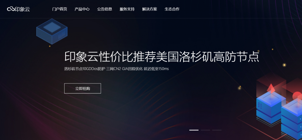
印象云七夕促销,所有机器7折销售,美国CERA低至18元/月 年付217元!
印象云,成立于2019年3月的商家,公司注册于中国香港,国人运行。目前主要从事美国CERA机房高防VPS以及香港三网CN2直连VPS和美国洛杉矶GIA三网线路服务器销售。印象云香港三网CN2机房,主要是CN2直连大陆,超低延迟!对于美国CERA机房应该不陌生,主要是做高防服务器产品的,并且此机房对中国大陆支持比较友好,印象云美国高防VPS服务器去程是163直连、三网回程CN2优化,单IP默认给20...
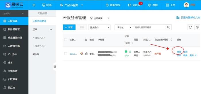
易探云服务器怎么过户/转让?云服务器PUSH实操步骤
易探云服务器怎么过户/转让?易探云支持云服务器PUSH功能,该功能可将云服务器过户给指定用户。可带价PUSH,收到PUSH请求的用户在接收云服务器的同时,系统会扣除接收方的款项,同时扣除相关手续费,然后将款项打到发送方的账户下。易探云“PUSH服务器”的这一功能,可以让用户将闲置云服务器转让给更多需要购买的用户!易探云服务器怎么过户/PUSH?1.PUSH双方必须为认证用户:2.买家未接收前,卖家...
韩国服务器租用优惠点评大全
韩国服务器怎么样?韩国云服务器租用推荐?韩国服务器距离中国近,有天然的地域优势,韩国服务器速度快而且非常稳定!有不少有亚洲市场的外贸公司选择韩国服务器开拓业务,韩国服务器因自身的优势也受到不少用户的青睐。目前的IDC市场上,韩国、香港、美国三个地方的服务器几乎占据了海外服务器的百分之九十以上。韩国服务器相比美国服务器来说速度更快,而相比香港机房来说则带宽更充足,占用市场份额非常大。那么,韩国服务器...

www.99cycy.com为你推荐
-
梦之队官网梦之队是什么呢?是那个国家的呢?他们又是参加那个项目的呢?得了几块金牌呢?access数据库access数据库主要学什么百度关键词价格查询如何查到推广关键词的价钱?同ip网站同IP的两个网站,做单向链接,会不会被K掉??mole.61.com摩尔大陆?????www.7788k.comwww.6601txq.com.有没有这个网站广告法广告法有什么字不能用javlibrary.com大家有没有在线图书馆WWW。QUESTIA。COM的免费帐号鹤城勿扰齐齐哈尔电视台晴彩鹤城是哪个频道ename.com趫 是什么意思?