FREQUENCYwww.765.com
www.765.com 时间:2021-03-19 阅读:()
DRV603www.
ti.
comSLOS617C–JANUARY2009–REVISEDNOVEMBER2009DirectPath,3-VRMSLineDriverWithAdjustableGainCheckforSamples:DRV6031FEATURESDESCRIPTION234DirectPathTheDRV603PWisa3-VRMSpop-freestereolinedriverdesignedtoallowtheremovaloftheoutput–EliminatesPop/Clicksdc-blockingcapacitorsforreducedcomponentcount–EliminatesOutputDC-BlockingCapacitorsandcost.
Thedeviceisidealforsingle-supply–ProvidesFlatFrequencyResponse20electronicswheresizeandcostarecriticaldesignHz–20kHzparameters.
LowNoiseandTHDDesignedusingTI'spatentedDirectPath–SNR>109dBtechnology,TheDRV603iscapableofdriving3Vrmsintoa2.
5-kloadwith5-Vsupplyvoltage.
The–TypicalVn600ENtoGND–0.
3toVDD+0.
3VTJMaximumoperatingjunctiontemperaturerange–40to150°CTstgStoragetemperaturerange–40to150°CESDElectrostaticdischarge,IECESDOUTL,OUTR±8kV(1)Stressesbeyondthoselistedunderabsolutemaximumratingsmaycausepermanentdamagetothedevice.
Thesearestressratingsonly,andfunctionaloperationofthedeviceattheseoranyotherconditionsbeyondthoseindicatedunderrecommendedoperatingconditionsisnotimplied.
Exposuretoabsolute-maximum-ratedconditionsforextendedperiodsmayaffectdevicereliability.
DISSIPATIONRATINGSPOWERRATING(1)POWERRATING(1)PACKAGERθJC(°C/W)RθJA(°C/W)ATTA≤25°CATTA≤70°CTSSOP-14(PW)35115(2)870mW348mW(1)Powerratingisdeterminedwithajunctiontemperatureof125°C.
Thisisthepointwhereperformancestartstodegradeandlong-termreliabilitystartstobereduced.
ThermalmanagementofthefinalPCBshouldstrivetokeepthejunctiontemperatureatorbelow125°Cforbestperformanceandreliability.
(2)ThesedataweretakenwiththeJEDEChigh-Ktestprintedcircuitboard(PCB).
FortheJEDEClow-KtestPCB,theRθJAis185°C/W.
RECOMMENDEDOPERATINGCONDITIONSMINNOMMAXUNITVDDSupplyvoltageDCsupplyvoltage33.
35.
5VVIHHigh-levelinputvoltageEN60%ofVDDVILLow-levelinputvoltageEN40%ofVDDTAOperatingfree-airtemperature070°C2SubmitDocumentationFeedbackCopyright2009,TexasInstrumentsIncorporatedProductFolderLink(s):DRV603DRV603www.
ti.
comSLOS617C–JANUARY2009–REVISEDNOVEMBER2009ELECTRICALCHARACTERISTICSTA=25°C(unlessotherwisenoted)PARAMETERTESTCONDITIONSMINTYPMAXUNIT|VOS|OutputoffsetvoltageVDD=3Vto5V,inputgrounded,unitygain1mVPSRRPower-supplyrejectionratioVDD=3Vto5V88dBVOHHigh-leveloutputvoltageVDD=3.
3V,RL=2.
5k3.
1VVOLLow-leveloutputvoltageVDD=3.
3V,RL=2.
5k–3.
05V|IIH|High-levelinputcurrent(EN)VDD=5V,VI=VDD1A|IIL|Low-levelinputcurrent(EN)VDD=5V,VI=0V1AVDD=3.
3V,noload,EN=VDD11IDDSupplycurrentVDD=5V,noload,EN=VDD12.
5mAShutdownmode,VDD=3Vto5V1OPERATINGCHARACTERISTICSVDD=3.
3V,TA=25°C,RL=2.
5k,C(PUMP)=C(PVSS)=1F,CIN=10F,RIN=10k,Rfb=20k(unlessotherwisenoted)PARAMETERTESTCONDITIONSMINTYPMAXUNITTHD=1%,VDD=3.
3V,f=1kHz2.
05VOOutputvoltage(outputsinphase)THD=1%,VDD=5V,f=1kHz3.
01VrmsTHD=1%,VDD=5V,f=1kHz,RL=100k3.
1THD+NTotalharmonicdistortionplusnoiseVO=2Vrms,f=1kHz0.
001%CrosstalkVO=2Vrms,f=1kHz–100dBIOMaximumoutputcurrentVDD=3.
3V20mARINInputresistorrange11047kRfbFeedbackresistorrange4.
720100kSlewrate4.
5V/μsMaximumcapacitiveload220pFVNNoiseoutputvoltageBW=20Hzto22kHz,A-weighted6μVrmsVO=3Vrms,THD+N=0.
1%,BW=22kHz,SNRSignal-to-noiseratio112dBA-weightedGBWUnity-gainbandwidth8MHzAVOOpen-loopvoltagegain150dBVuvpExternalundervoltagedetection1.
25VExternalundervoltagedetectionIHys5μAhysteresiscurrentfcpChargepumpfrequency225450675kHzCopyright2009,TexasInstrumentsIncorporatedSubmitDocumentationFeedback3ProductFolderLink(s):DRV603DRV603SLOS617C–JANUARY2009–REVISEDNOVEMBER2009www.
ti.
comPWPACKAGE(TOPVIEW)PINFUNCTIONSPINI/O(1)DESCRIPTIONNAMENO.
+INR1IRight-channelOPAMPpositiveinput–INR2IRight-channelOPAMPnegativeinputOUTR3ORight-channelOPAMPoutputSGND4PSignalgroundEN5IEnableinput,active-highPVSS6PSupplyvoltageCN7I/OCharge-pumpflyingcapacitornegativeterminalCP8I/OCharge-pumpflyingcapacitorpositiveterminalPVDD9PPositivesupplyPGND10PPowergroundUVP11IUndervoltageprotectioninputOUTL12OLeft-channelOPAMPoutput–INL13ILeft-channelOPAMPnegativeinput+INL14ILeft-channelOPAMPpositiveinput(1)I=input,O=output,P=power4SubmitDocumentationFeedbackCopyright2009,TexasInstrumentsIncorporatedProductFolderLink(s):DRV603DRV603www.
ti.
comSLOS617C–JANUARY2009–REVISEDNOVEMBER2009FUNCTIONALBLOCKDIAGRAMCopyright2009,TexasInstrumentsIncorporatedSubmitDocumentationFeedback5ProductFolderLink(s):DRV603DRV603SLOS617C–JANUARY2009–REVISEDNOVEMBER2009www.
ti.
comTYPICALCHARACTERISTICSVDD=3.
3V,TA=25°C,RL=2.
5k,C(PUMP)=C(VSS)=1F,CIN=10F,RIN=10k,Rfb=20k(unlessotherwisenoted)TOTALHARMONICDISTORTION+NOISETOTALHARMONICDISTORTION+NOISEvsvsOUTPUTVOLTAGEOUTPUTVOLTAGEVDD=3.
3V,RL=100k,f=1kHzVDD=5V,RL=100k,f=1kHzFigure1.
Figure2.
TOTALHARMONICDISTORTION+NOISETOTALHARMONICDISTORTION+NOISEvsvsOUTPUTVOLTAGEOUTPUTVOLTAGEVDD=3.
3V,RL=2.
5k,f=1kHzVDD=5V,RL=600,f=1kHzFigure3.
Figure4.
6SubmitDocumentationFeedbackCopyright2009,TexasInstrumentsIncorporatedProductFolderLink(s):DRV603DRV603www.
ti.
comSLOS617C–JANUARY2009–REVISEDNOVEMBER2009TYPICALCHARACTERISTICS(continued)VDD=3.
3V,TA=25°C,RL=2.
5k,C(PUMP)=C(VSS)=1F,CIN=10F,RIN=10k,Rfb=20k(unlessotherwisenoted)TOTALHARMONICDISTORTION+NOISETOTALHARMONICDISTORTION+NOISEvsvsFREQUENCYFREQUENCYVDD=3.
3V,RL=2.
5k,VO=2VrmsVDD=5V,RL=100k,VO=2VrmsFigure5.
Figure6.
PHASEGAINvsvsFREQUENCYFREQUENCYVDD=5V,RL=100k,VO=2VrmsVDD=5V,RL=100k,VO=2VrmsFigure7.
Figure8.
Copyright2009,TexasInstrumentsIncorporatedSubmitDocumentationFeedback7ProductFolderLink(s):DRV603DRV603SLOS617C–JANUARY2009–REVISEDNOVEMBER2009www.
ti.
comTYPICALCHARACTERISTICS(continued)VDD=3.
3V,TA=25°C,RL=2.
5k,C(PUMP)=C(VSS)=1F,CIN=10F,RIN=10k,Rfb=20k(unlessotherwisenoted)FFTvsQUIESCENTCURRENTFREQUENCYvsVDD=5V,RL=100k,VO=3Vrms(-60dB)SUPPLYVOLTAGEFigure9.
Figure10.
8SubmitDocumentationFeedbackCopyright2009,TexasInstrumentsIncorporatedProductFolderLink(s):DRV603DRV603www.
ti.
comSLOS617C–JANUARY2009–REVISEDNOVEMBER2009APPLICATIONINFORMATIONLINEDRIVERAMPLIFIERSSingle-supplyline-driveramplifierstypicallyrequiredc-blockingcapacitors.
ThetopdrawinginFigure11illustratestheconventionalline-driveramplifierconnectiontotheloadandoutputsignal.
DCblockingcapacitorsareoftenlargeinvalue,andamutecircuitisneededduringpoweruptominimizeclickandpop.
TheoutputcapacitorandmutecircuitconsumePCBareaandincreasecostofassembly,andcanreducethefidelityoftheaudiooutputsignal.
Figure11.
ConventionalandDirectPathLineDriverTheDirectPathamplifierarchitectureoperatesfromasinglesupplybutmakesuseofaninternalchargepumptoprovideanegativevoltagerail.
Combiningtheuser-providedpositiverailandthenegativerailgeneratedbytheIC,thedeviceoperatesinwhatiseffectivelyasplitsupplymode.
Theoutputvoltagesarenowcenteredatzerovoltswiththecapabilitytoswingtothepositiverailornegativerail.
Combiningthiswiththebuilt-inclickandpopreductioncircuit,theDirectPathamplifierrequiresnooutputdcblockingcapacitors.
ThebottomblockdiagramandwaveformofFigure11illustratetheground-referencedline-driverarchitecture.
ThisisthearchitectureoftheDRV603.
Copyright2009,TexasInstrumentsIncorporatedSubmitDocumentationFeedback9ProductFolderLink(s):DRV603DRV603SLOS617C–JANUARY2009–REVISEDNOVEMBER2009www.
ti.
comCHARGEPUMPFLYINGCAPACITORANDPVSSCAPACITORThechargepumpflyingcapacitorservestotransferchargeduringthegenerationofthenegativesupplyvoltage.
ThePVSScapacitormustbeatleastequaltothechargepumpcapacitorinordertoallowmaximumchargetransfer.
Low-ESRcapacitorsareanidealselection,andavalueof1μFistypical.
Capacitorvaluesthataresmallerthan1μFcanbeused,butthemaximumoutputvoltagemaybereducedandthedevicemaynotoperatetospecifications.
DECOUPLINGCAPACITORSTheDRV603isaDirectPathline-driveramplifierthatrequiresadequatepowersupplydecouplingtoensurethatthenoiseandtotalharmonicdistortion(THD)arelow.
Agoodlowequivalent-series-resistance(ESR)ceramiccapacitor,typically1μF,placedascloseaspossibletothedeviceVDDleadworksbest.
PlacingthisdecouplingcapacitorclosetotheDRV603isimportantfortheperformanceoftheamplifier.
Forfilteringlower-frequencynoisesignals,a10-μForgreatercapacitorplacedneartheaudiopoweramplifierwouldalsohelp,butitisnotrequiredinmostapplicationsbecauseofthehighPSRRofthisdevice.
GAIN-SETTINGRESISTORRANGESThegain-settingresistors,RINandRfb,mustbechosensothatnoise,stability,andinputcapacitorsizeoftheDRV603arekeptwithinacceptablelimits.
VoltagegainisdefinedasRfbdividedbyRIN.
Selectingvaluesthataretoolowdemandsalargeinputac-couplingcapacitor,CIN.
Selectingvaluesthataretoohighincreasesthenoiseoftheamplifier.
Table1liststherecommendedresistorvaluesfordifferentgainsettings.
Table1.
RecommendedResistorValuesINPUTRESISTORFEEDBACKRESISTORDIFFERENTIALINPUTNONINVERTINGINPUTINVERTINGINPUTGAINVALUE,RINVALUE,RfbGAINGAIN22k22k1V/V–1V/V2V/V15k30k1.
5V/V–1.
5V/V2.
5V/V33k68k2.
1V/V–2.
1V/V3.
1V/V10k100k10V/V–10V/V11V/VFigure12.
Differential,InvertingandNon-InvertingGainConfigurations10SubmitDocumentationFeedbackCopyright2009,TexasInstrumentsIncorporatedProductFolderLink(s):DRV603DRV603www.
ti.
comSLOS617C–JANUARY2009–REVISEDNOVEMBER2009INPUT-BLOCKINGCAPACITORSDCinput-blockingcapacitorsarerequiredtobeaddedinserieswiththeaudiosignalintotheinputpinsoftheDRV603.
ThesecapacitorsblockthedcportionoftheaudiosourceandallowtheDRV603inputstobeproperlybiasedtoprovidemaximumperformance.
Thesecapacitorsformahigh-passfilterwiththeinputresistor,RIN.
ThecutofffrequencyiscalculatedusingEquation1.
Forthiscalculation,thecapacitanceusedistheinput-blockingcapacitorandtheresistanceistheinputresistorchosenfromTable1.
Thenthefrequencyand/orcapacitancecanbedeterminedwhenoneofthetwovaluesisgiven.
(1)USINGTHEDRV603ASASECOND-ORDERFILTERSeveralaudioDACsusedtodayrequireanexternallow-passfiltertoremoveout-of-bandnoise.
ThisispossiblewiththeDRV603,asitcanbeusedlikeastandardOPAMP.
Severalfiltertopologiescanbeimplemented,bothsingle-endedanddifferential.
InFigure13,amulti-feedback(MFB)withdifferentialinputandsingle-endedinputisshown.
Anac-couplingcapacitortoremovedccontentfromthesourceisshown;itservestoblockanydccontentfromthesourceandlowersthedc-gainto1,helpingreducingtheoutputdc-offsettominimum.
ThecomponentvaluescanbecalculatedwiththehelpoftheTIFilterProprogramavailableontheTIwebsiteat:http://focus.
ti.
com/docs/toolsw/folders/print/filterpro.
htmlFigure13.
Second-OrderActiveLow-PassFilterTheresistorvaluesshouldhavealowvalueforobtaininglownoise,butshouldalsohaveahighenoughvaluetogetasmallsizeac-couplingcapacitor.
Using5.
6kΩfortheresistors,C1=220pF,andC2=470pF,aDNRof112dBcanbeachievedwitha10-μFinputac-couplingcapacitor.
Copyright2009,TexasInstrumentsIncorporatedSubmitDocumentationFeedback11ProductFolderLink(s):DRV603DRV603SLOS617C–JANUARY2009–REVISEDNOVEMBER2009www.
ti.
comPOP-FREEPOWERUPPop-freepowerupisensuredbykeepingtheSD(shutdownpin)lowduringpower-supplyrampupandrampdown.
TheSDpinshouldbekeptlowuntiltheinputac-couplingcapacitorsarefullychargedbeforeassertingtheSDpinhightoachievepop-lesspowerup.
Figure14illustratesthepreferredsequence.
Figure14.
Power-UpSequenceEXTERNALUNDERVOLTAGEDETECTIONExternalundervoltagedetectioncanbeusedtomute/shutdowntheDRV603beforeaninputdevicecangenerateapop.
TheshutdownthresholdattheUVPpinis1.
25V.
Theuserselectsaresistordividertoobtaintheshutdownthresholdandhysteresisforthespecificapplication.
Thethresholdscanbedeterminedasfollows:VUVP=1.
25V*(R11+R12)/R12Hysteresis=5μA*R13*(R11+R12)/R12withtheconditionR13>>R11//R12.
Forexample,toobtainVUVP=5Vand1-Vhysteresis,R11=3k,R12=1kandR13=50k.
CAPACITIVELOADTheDRV603hastheabilitytodriveahighcapacitiveloadupto220pFdirectly.
Highercapacitiveloadscanbeacceptedbyaddingaseriesresistorof47orlarger.
LAYOUTRECOMMENDATIONSAproposedlayoutfortheDRV603canbeseenintheDRV603EVMUser'sGuide(SLOU248),andtheGerberfilescanbedownloadedfromhttp://focus.
ti.
com/docs/toolsw/folders/print/drv603evm.
html.
Toaccessthisinformation,opentheDRV603productfolderandlookintheToolsandSoftwarefolder.
GAIN-SETTINGRESISTORSThegain-settingresistors,RINandRfb,mustbeplacedclosetotheinputpinstominimizecapacitiveloadingontheseinputpinsandtoensuremaximumstabilityoftheDRV603.
FortherecommendedPCBlayout,seetheDRV603EVMuser'sguide(SLOU248).
12SubmitDocumentationFeedbackCopyright2009,TexasInstrumentsIncorporatedProductFolderLink(s):DRV603DRV603www.
ti.
comSLOS617C–JANUARY2009–REVISEDNOVEMBER2009APPLICATIONCIRCUITR1=5.
6k,R2=5.
6k,R3=5.
6k,C1=220pF,C2=470pFDifferential-input,single-endedoutput,second-orderfilterCopyright2009,TexasInstrumentsIncorporatedSubmitDocumentationFeedback13ProductFolderLink(s):DRV603DRV603SLOS617C–JANUARY2009–REVISEDNOVEMBER2009www.
ti.
comREVISIONHISTORYNOTE:Pagenumbersofcurrentversionmaydifferfrompreviousversions.
ChangesfromRevisionA(February2009)toRevisionBPageChangedCrosstalkspecfrom–80dBto–100dB3Addedmissingvoltagevalue(1.
25V)toExternalUndervoltageDetectionthresholdequation.
1214SubmitDocumentationFeedbackCopyright2009,TexasInstrumentsIncorporatedProductFolderLink(s):DRV603DRV603www.
ti.
comSLOS617C–JANUARY2009–REVISEDNOVEMBER2009ChangesfromRevisionB(October2009)toRevisionCPageChangedmaximumoperatingjunctiontemperature2InDissipationRatingssection,changedθJxtoRθJxinthreeplacesand185°Cto185°C/W2CorrectedreferencetoFigure119Addedcross-referencetoFigure1311Copyright2009,TexasInstrumentsIncorporatedSubmitDocumentationFeedback15ProductFolderLink(s):DRV603PACKAGEOPTIONADDENDUMwww.
ti.
com10-Dec-2020Addendum-Page1PACKAGINGINFORMATIONOrderableDeviceStatus(1)PackageTypePackageDrawingPinsPackageQtyEcoPlan(2)Leadfinish/Ballmaterial(6)MSLPeakTemp(3)OpTemp(°C)DeviceMarking(4/5)SamplesDRV603PWACTIVETSSOPPW1490RoHS&GreenNIPDAULevel-1-260C-UNLIM-40to85DRV603DRV603PWRACTIVETSSOPPW142000RoHS&GreenNIPDAULevel-1-260C-UNLIM-40to85DRV603(1)Themarketingstatusvaluesaredefinedasfollows:ACTIVE:Productdevicerecommendedfornewdesigns.
LIFEBUY:TIhasannouncedthatthedevicewillbediscontinued,andalifetime-buyperiodisineffect.
NRND:Notrecommendedfornewdesigns.
Deviceisinproductiontosupportexistingcustomers,butTIdoesnotrecommendusingthispartinanewdesign.
PREVIEW:Devicehasbeenannouncedbutisnotinproduction.
Samplesmayormaynotbeavailable.
OBSOLETE:TIhasdiscontinuedtheproductionofthedevice.
(2)RoHS:TIdefines"RoHS"tomeansemiconductorproductsthatarecompliantwiththecurrentEURoHSrequirementsforall10RoHSsubstances,includingtherequirementthatRoHSsubstancedonotexceed0.
1%byweightinhomogeneousmaterials.
Wheredesignedtobesolderedathightemperatures,"RoHS"productsaresuitableforuseinspecifiedlead-freeprocesses.
TImayreferencethesetypesofproductsas"Pb-Free".
RoHSExempt:TIdefines"RoHSExempt"tomeanproductsthatcontainleadbutarecompliantwithEURoHSpursuanttoaspecificEURoHSexemption.
Green:TIdefines"Green"tomeanthecontentofChlorine(Cl)andBromine(Br)basedflameretardantsmeetJS709Blowhalogenrequirementsof<=1000ppmthreshold.
Antimonytrioxidebasedflameretardantsmustalsomeetthe<=1000ppmthresholdrequirement.
(3)MSL,PeakTemp.
-TheMoistureSensitivityLevelratingaccordingtotheJEDECindustrystandardclassifications,andpeaksoldertemperature.
(4)Theremaybeadditionalmarking,whichrelatestothelogo,thelottracecodeinformation,ortheenvironmentalcategoryonthedevice.
(5)MultipleDeviceMarkingswillbeinsideparentheses.
OnlyoneDeviceMarkingcontainedinparenthesesandseparatedbya"~"willappearonadevice.
IfalineisindentedthenitisacontinuationofthepreviouslineandthetwocombinedrepresenttheentireDeviceMarkingforthatdevice.
(6)Leadfinish/Ballmaterial-OrderableDevicesmayhavemultiplematerialfinishoptions.
Finishoptionsareseparatedbyaverticalruledline.
Leadfinish/Ballmaterialvaluesmaywraptotwolinesifthefinishvalueexceedsthemaximumcolumnwidth.
ImportantInformationandDisclaimer:TheinformationprovidedonthispagerepresentsTI'sknowledgeandbeliefasofthedatethatitisprovided.
TIbasesitsknowledgeandbeliefoninformationprovidedbythirdparties,andmakesnorepresentationorwarrantyastotheaccuracyofsuchinformation.
Effortsareunderwaytobetterintegrateinformationfromthirdparties.
TIhastakenandcontinuestotakereasonablestepstoproviderepresentativeandaccurateinformationbutmaynothaveconducteddestructivetestingorchemicalanalysisonincomingmaterialsandchemicals.
TIandTIsuppliersconsidercertaininformationtobeproprietary,andthusCASnumbersandotherlimitedinformationmaynotbeavailableforrelease.
InnoeventshallTI'sliabilityarisingoutofsuchinformationexceedthetotalpurchasepriceoftheTIpart(s)atissueinthisdocumentsoldbyTItoCustomeronanannualbasis.
PACKAGEOPTIONADDENDUMwww.
ti.
com10-Dec-2020Addendum-Page2TAPEANDREELINFORMATION*AlldimensionsarenominalDevicePackageTypePackageDrawingPinsSPQReelDiameter(mm)ReelWidthW1(mm)A0(mm)B0(mm)K0(mm)P1(mm)W(mm)Pin1QuadrantDRV603PWRTSSOPPW142000330.
012.
46.
95.
61.
68.
012.
0Q1PACKAGEMATERIALSINFORMATIONwww.
ti.
com26-Feb-2019PackMaterials-Page1*AlldimensionsarenominalDevicePackageTypePackageDrawingPinsSPQLength(mm)Width(mm)Height(mm)DRV603PWRTSSOPPW142000350.
0350.
043.
0PACKAGEMATERIALSINFORMATIONwww.
ti.
com26-Feb-2019PackMaterials-Page2IMPORTANTNOTICEANDDISCLAIMERTIPROVIDESTECHNICALANDRELIABILITYDATA(INCLUDINGDATASHEETS),DESIGNRESOURCES(INCLUDINGREFERENCEDESIGNS),APPLICATIONOROTHERDESIGNADVICE,WEBTOOLS,SAFETYINFORMATION,ANDOTHERRESOURCES"ASIS"ANDWITHALLFAULTS,ANDDISCLAIMSALLWARRANTIES,EXPRESSANDIMPLIED,INCLUDINGWITHOUTLIMITATIONANYIMPLIEDWARRANTIESOFMERCHANTABILITY,FITNESSFORAPARTICULARPURPOSEORNON-INFRINGEMENTOFTHIRDPARTYINTELLECTUALPROPERTYRIGHTS.
TheseresourcesareintendedforskilleddevelopersdesigningwithTIproducts.
Youaresolelyresponsiblefor(1)selectingtheappropriateTIproductsforyourapplication,(2)designing,validatingandtestingyourapplication,and(3)ensuringyourapplicationmeetsapplicablestandards,andanyothersafety,security,orotherrequirements.
Theseresourcesaresubjecttochangewithoutnotice.
TIgrantsyoupermissiontousetheseresourcesonlyfordevelopmentofanapplicationthatusestheTIproductsdescribedintheresource.
Otherreproductionanddisplayoftheseresourcesisprohibited.
NolicenseisgrantedtoanyotherTIintellectualpropertyrightortoanythirdpartyintellectualpropertyright.
TIdisclaimsresponsibilityfor,andyouwillfullyindemnifyTIanditsrepresentativesagainst,anyclaims,damages,costs,losses,andliabilitiesarisingoutofyouruseoftheseresources.
TI'sproductsareprovidedsubjecttoTI'sTermsofSale(www.
ti.
com/legal/termsofsale.
html)orotherapplicabletermsavailableeitheronti.
comorprovidedinconjunctionwithsuchTIproducts.
TI'sprovisionoftheseresourcesdoesnotexpandorotherwisealterTI'sapplicablewarrantiesorwarrantydisclaimersforTIproducts.
MailingAddress:TexasInstruments,PostOfficeBox655303,Dallas,Texas75265Copyright2020,TexasInstrumentsIncorporated
ti.
comSLOS617C–JANUARY2009–REVISEDNOVEMBER2009DirectPath,3-VRMSLineDriverWithAdjustableGainCheckforSamples:DRV6031FEATURESDESCRIPTION234DirectPathTheDRV603PWisa3-VRMSpop-freestereolinedriverdesignedtoallowtheremovaloftheoutput–EliminatesPop/Clicksdc-blockingcapacitorsforreducedcomponentcount–EliminatesOutputDC-BlockingCapacitorsandcost.
Thedeviceisidealforsingle-supply–ProvidesFlatFrequencyResponse20electronicswheresizeandcostarecriticaldesignHz–20kHzparameters.
LowNoiseandTHDDesignedusingTI'spatentedDirectPath–SNR>109dBtechnology,TheDRV603iscapableofdriving3Vrmsintoa2.
5-kloadwith5-Vsupplyvoltage.
The–TypicalVn600ENtoGND–0.
3toVDD+0.
3VTJMaximumoperatingjunctiontemperaturerange–40to150°CTstgStoragetemperaturerange–40to150°CESDElectrostaticdischarge,IECESDOUTL,OUTR±8kV(1)Stressesbeyondthoselistedunderabsolutemaximumratingsmaycausepermanentdamagetothedevice.
Thesearestressratingsonly,andfunctionaloperationofthedeviceattheseoranyotherconditionsbeyondthoseindicatedunderrecommendedoperatingconditionsisnotimplied.
Exposuretoabsolute-maximum-ratedconditionsforextendedperiodsmayaffectdevicereliability.
DISSIPATIONRATINGSPOWERRATING(1)POWERRATING(1)PACKAGERθJC(°C/W)RθJA(°C/W)ATTA≤25°CATTA≤70°CTSSOP-14(PW)35115(2)870mW348mW(1)Powerratingisdeterminedwithajunctiontemperatureof125°C.
Thisisthepointwhereperformancestartstodegradeandlong-termreliabilitystartstobereduced.
ThermalmanagementofthefinalPCBshouldstrivetokeepthejunctiontemperatureatorbelow125°Cforbestperformanceandreliability.
(2)ThesedataweretakenwiththeJEDEChigh-Ktestprintedcircuitboard(PCB).
FortheJEDEClow-KtestPCB,theRθJAis185°C/W.
RECOMMENDEDOPERATINGCONDITIONSMINNOMMAXUNITVDDSupplyvoltageDCsupplyvoltage33.
35.
5VVIHHigh-levelinputvoltageEN60%ofVDDVILLow-levelinputvoltageEN40%ofVDDTAOperatingfree-airtemperature070°C2SubmitDocumentationFeedbackCopyright2009,TexasInstrumentsIncorporatedProductFolderLink(s):DRV603DRV603www.
ti.
comSLOS617C–JANUARY2009–REVISEDNOVEMBER2009ELECTRICALCHARACTERISTICSTA=25°C(unlessotherwisenoted)PARAMETERTESTCONDITIONSMINTYPMAXUNIT|VOS|OutputoffsetvoltageVDD=3Vto5V,inputgrounded,unitygain1mVPSRRPower-supplyrejectionratioVDD=3Vto5V88dBVOHHigh-leveloutputvoltageVDD=3.
3V,RL=2.
5k3.
1VVOLLow-leveloutputvoltageVDD=3.
3V,RL=2.
5k–3.
05V|IIH|High-levelinputcurrent(EN)VDD=5V,VI=VDD1A|IIL|Low-levelinputcurrent(EN)VDD=5V,VI=0V1AVDD=3.
3V,noload,EN=VDD11IDDSupplycurrentVDD=5V,noload,EN=VDD12.
5mAShutdownmode,VDD=3Vto5V1OPERATINGCHARACTERISTICSVDD=3.
3V,TA=25°C,RL=2.
5k,C(PUMP)=C(PVSS)=1F,CIN=10F,RIN=10k,Rfb=20k(unlessotherwisenoted)PARAMETERTESTCONDITIONSMINTYPMAXUNITTHD=1%,VDD=3.
3V,f=1kHz2.
05VOOutputvoltage(outputsinphase)THD=1%,VDD=5V,f=1kHz3.
01VrmsTHD=1%,VDD=5V,f=1kHz,RL=100k3.
1THD+NTotalharmonicdistortionplusnoiseVO=2Vrms,f=1kHz0.
001%CrosstalkVO=2Vrms,f=1kHz–100dBIOMaximumoutputcurrentVDD=3.
3V20mARINInputresistorrange11047kRfbFeedbackresistorrange4.
720100kSlewrate4.
5V/μsMaximumcapacitiveload220pFVNNoiseoutputvoltageBW=20Hzto22kHz,A-weighted6μVrmsVO=3Vrms,THD+N=0.
1%,BW=22kHz,SNRSignal-to-noiseratio112dBA-weightedGBWUnity-gainbandwidth8MHzAVOOpen-loopvoltagegain150dBVuvpExternalundervoltagedetection1.
25VExternalundervoltagedetectionIHys5μAhysteresiscurrentfcpChargepumpfrequency225450675kHzCopyright2009,TexasInstrumentsIncorporatedSubmitDocumentationFeedback3ProductFolderLink(s):DRV603DRV603SLOS617C–JANUARY2009–REVISEDNOVEMBER2009www.
ti.
comPWPACKAGE(TOPVIEW)PINFUNCTIONSPINI/O(1)DESCRIPTIONNAMENO.
+INR1IRight-channelOPAMPpositiveinput–INR2IRight-channelOPAMPnegativeinputOUTR3ORight-channelOPAMPoutputSGND4PSignalgroundEN5IEnableinput,active-highPVSS6PSupplyvoltageCN7I/OCharge-pumpflyingcapacitornegativeterminalCP8I/OCharge-pumpflyingcapacitorpositiveterminalPVDD9PPositivesupplyPGND10PPowergroundUVP11IUndervoltageprotectioninputOUTL12OLeft-channelOPAMPoutput–INL13ILeft-channelOPAMPnegativeinput+INL14ILeft-channelOPAMPpositiveinput(1)I=input,O=output,P=power4SubmitDocumentationFeedbackCopyright2009,TexasInstrumentsIncorporatedProductFolderLink(s):DRV603DRV603www.
ti.
comSLOS617C–JANUARY2009–REVISEDNOVEMBER2009FUNCTIONALBLOCKDIAGRAMCopyright2009,TexasInstrumentsIncorporatedSubmitDocumentationFeedback5ProductFolderLink(s):DRV603DRV603SLOS617C–JANUARY2009–REVISEDNOVEMBER2009www.
ti.
comTYPICALCHARACTERISTICSVDD=3.
3V,TA=25°C,RL=2.
5k,C(PUMP)=C(VSS)=1F,CIN=10F,RIN=10k,Rfb=20k(unlessotherwisenoted)TOTALHARMONICDISTORTION+NOISETOTALHARMONICDISTORTION+NOISEvsvsOUTPUTVOLTAGEOUTPUTVOLTAGEVDD=3.
3V,RL=100k,f=1kHzVDD=5V,RL=100k,f=1kHzFigure1.
Figure2.
TOTALHARMONICDISTORTION+NOISETOTALHARMONICDISTORTION+NOISEvsvsOUTPUTVOLTAGEOUTPUTVOLTAGEVDD=3.
3V,RL=2.
5k,f=1kHzVDD=5V,RL=600,f=1kHzFigure3.
Figure4.
6SubmitDocumentationFeedbackCopyright2009,TexasInstrumentsIncorporatedProductFolderLink(s):DRV603DRV603www.
ti.
comSLOS617C–JANUARY2009–REVISEDNOVEMBER2009TYPICALCHARACTERISTICS(continued)VDD=3.
3V,TA=25°C,RL=2.
5k,C(PUMP)=C(VSS)=1F,CIN=10F,RIN=10k,Rfb=20k(unlessotherwisenoted)TOTALHARMONICDISTORTION+NOISETOTALHARMONICDISTORTION+NOISEvsvsFREQUENCYFREQUENCYVDD=3.
3V,RL=2.
5k,VO=2VrmsVDD=5V,RL=100k,VO=2VrmsFigure5.
Figure6.
PHASEGAINvsvsFREQUENCYFREQUENCYVDD=5V,RL=100k,VO=2VrmsVDD=5V,RL=100k,VO=2VrmsFigure7.
Figure8.
Copyright2009,TexasInstrumentsIncorporatedSubmitDocumentationFeedback7ProductFolderLink(s):DRV603DRV603SLOS617C–JANUARY2009–REVISEDNOVEMBER2009www.
ti.
comTYPICALCHARACTERISTICS(continued)VDD=3.
3V,TA=25°C,RL=2.
5k,C(PUMP)=C(VSS)=1F,CIN=10F,RIN=10k,Rfb=20k(unlessotherwisenoted)FFTvsQUIESCENTCURRENTFREQUENCYvsVDD=5V,RL=100k,VO=3Vrms(-60dB)SUPPLYVOLTAGEFigure9.
Figure10.
8SubmitDocumentationFeedbackCopyright2009,TexasInstrumentsIncorporatedProductFolderLink(s):DRV603DRV603www.
ti.
comSLOS617C–JANUARY2009–REVISEDNOVEMBER2009APPLICATIONINFORMATIONLINEDRIVERAMPLIFIERSSingle-supplyline-driveramplifierstypicallyrequiredc-blockingcapacitors.
ThetopdrawinginFigure11illustratestheconventionalline-driveramplifierconnectiontotheloadandoutputsignal.
DCblockingcapacitorsareoftenlargeinvalue,andamutecircuitisneededduringpoweruptominimizeclickandpop.
TheoutputcapacitorandmutecircuitconsumePCBareaandincreasecostofassembly,andcanreducethefidelityoftheaudiooutputsignal.
Figure11.
ConventionalandDirectPathLineDriverTheDirectPathamplifierarchitectureoperatesfromasinglesupplybutmakesuseofaninternalchargepumptoprovideanegativevoltagerail.
Combiningtheuser-providedpositiverailandthenegativerailgeneratedbytheIC,thedeviceoperatesinwhatiseffectivelyasplitsupplymode.
Theoutputvoltagesarenowcenteredatzerovoltswiththecapabilitytoswingtothepositiverailornegativerail.
Combiningthiswiththebuilt-inclickandpopreductioncircuit,theDirectPathamplifierrequiresnooutputdcblockingcapacitors.
ThebottomblockdiagramandwaveformofFigure11illustratetheground-referencedline-driverarchitecture.
ThisisthearchitectureoftheDRV603.
Copyright2009,TexasInstrumentsIncorporatedSubmitDocumentationFeedback9ProductFolderLink(s):DRV603DRV603SLOS617C–JANUARY2009–REVISEDNOVEMBER2009www.
ti.
comCHARGEPUMPFLYINGCAPACITORANDPVSSCAPACITORThechargepumpflyingcapacitorservestotransferchargeduringthegenerationofthenegativesupplyvoltage.
ThePVSScapacitormustbeatleastequaltothechargepumpcapacitorinordertoallowmaximumchargetransfer.
Low-ESRcapacitorsareanidealselection,andavalueof1μFistypical.
Capacitorvaluesthataresmallerthan1μFcanbeused,butthemaximumoutputvoltagemaybereducedandthedevicemaynotoperatetospecifications.
DECOUPLINGCAPACITORSTheDRV603isaDirectPathline-driveramplifierthatrequiresadequatepowersupplydecouplingtoensurethatthenoiseandtotalharmonicdistortion(THD)arelow.
Agoodlowequivalent-series-resistance(ESR)ceramiccapacitor,typically1μF,placedascloseaspossibletothedeviceVDDleadworksbest.
PlacingthisdecouplingcapacitorclosetotheDRV603isimportantfortheperformanceoftheamplifier.
Forfilteringlower-frequencynoisesignals,a10-μForgreatercapacitorplacedneartheaudiopoweramplifierwouldalsohelp,butitisnotrequiredinmostapplicationsbecauseofthehighPSRRofthisdevice.
GAIN-SETTINGRESISTORRANGESThegain-settingresistors,RINandRfb,mustbechosensothatnoise,stability,andinputcapacitorsizeoftheDRV603arekeptwithinacceptablelimits.
VoltagegainisdefinedasRfbdividedbyRIN.
Selectingvaluesthataretoolowdemandsalargeinputac-couplingcapacitor,CIN.
Selectingvaluesthataretoohighincreasesthenoiseoftheamplifier.
Table1liststherecommendedresistorvaluesfordifferentgainsettings.
Table1.
RecommendedResistorValuesINPUTRESISTORFEEDBACKRESISTORDIFFERENTIALINPUTNONINVERTINGINPUTINVERTINGINPUTGAINVALUE,RINVALUE,RfbGAINGAIN22k22k1V/V–1V/V2V/V15k30k1.
5V/V–1.
5V/V2.
5V/V33k68k2.
1V/V–2.
1V/V3.
1V/V10k100k10V/V–10V/V11V/VFigure12.
Differential,InvertingandNon-InvertingGainConfigurations10SubmitDocumentationFeedbackCopyright2009,TexasInstrumentsIncorporatedProductFolderLink(s):DRV603DRV603www.
ti.
comSLOS617C–JANUARY2009–REVISEDNOVEMBER2009INPUT-BLOCKINGCAPACITORSDCinput-blockingcapacitorsarerequiredtobeaddedinserieswiththeaudiosignalintotheinputpinsoftheDRV603.
ThesecapacitorsblockthedcportionoftheaudiosourceandallowtheDRV603inputstobeproperlybiasedtoprovidemaximumperformance.
Thesecapacitorsformahigh-passfilterwiththeinputresistor,RIN.
ThecutofffrequencyiscalculatedusingEquation1.
Forthiscalculation,thecapacitanceusedistheinput-blockingcapacitorandtheresistanceistheinputresistorchosenfromTable1.
Thenthefrequencyand/orcapacitancecanbedeterminedwhenoneofthetwovaluesisgiven.
(1)USINGTHEDRV603ASASECOND-ORDERFILTERSeveralaudioDACsusedtodayrequireanexternallow-passfiltertoremoveout-of-bandnoise.
ThisispossiblewiththeDRV603,asitcanbeusedlikeastandardOPAMP.
Severalfiltertopologiescanbeimplemented,bothsingle-endedanddifferential.
InFigure13,amulti-feedback(MFB)withdifferentialinputandsingle-endedinputisshown.
Anac-couplingcapacitortoremovedccontentfromthesourceisshown;itservestoblockanydccontentfromthesourceandlowersthedc-gainto1,helpingreducingtheoutputdc-offsettominimum.
ThecomponentvaluescanbecalculatedwiththehelpoftheTIFilterProprogramavailableontheTIwebsiteat:http://focus.
ti.
com/docs/toolsw/folders/print/filterpro.
htmlFigure13.
Second-OrderActiveLow-PassFilterTheresistorvaluesshouldhavealowvalueforobtaininglownoise,butshouldalsohaveahighenoughvaluetogetasmallsizeac-couplingcapacitor.
Using5.
6kΩfortheresistors,C1=220pF,andC2=470pF,aDNRof112dBcanbeachievedwitha10-μFinputac-couplingcapacitor.
Copyright2009,TexasInstrumentsIncorporatedSubmitDocumentationFeedback11ProductFolderLink(s):DRV603DRV603SLOS617C–JANUARY2009–REVISEDNOVEMBER2009www.
ti.
comPOP-FREEPOWERUPPop-freepowerupisensuredbykeepingtheSD(shutdownpin)lowduringpower-supplyrampupandrampdown.
TheSDpinshouldbekeptlowuntiltheinputac-couplingcapacitorsarefullychargedbeforeassertingtheSDpinhightoachievepop-lesspowerup.
Figure14illustratesthepreferredsequence.
Figure14.
Power-UpSequenceEXTERNALUNDERVOLTAGEDETECTIONExternalundervoltagedetectioncanbeusedtomute/shutdowntheDRV603beforeaninputdevicecangenerateapop.
TheshutdownthresholdattheUVPpinis1.
25V.
Theuserselectsaresistordividertoobtaintheshutdownthresholdandhysteresisforthespecificapplication.
Thethresholdscanbedeterminedasfollows:VUVP=1.
25V*(R11+R12)/R12Hysteresis=5μA*R13*(R11+R12)/R12withtheconditionR13>>R11//R12.
Forexample,toobtainVUVP=5Vand1-Vhysteresis,R11=3k,R12=1kandR13=50k.
CAPACITIVELOADTheDRV603hastheabilitytodriveahighcapacitiveloadupto220pFdirectly.
Highercapacitiveloadscanbeacceptedbyaddingaseriesresistorof47orlarger.
LAYOUTRECOMMENDATIONSAproposedlayoutfortheDRV603canbeseenintheDRV603EVMUser'sGuide(SLOU248),andtheGerberfilescanbedownloadedfromhttp://focus.
ti.
com/docs/toolsw/folders/print/drv603evm.
html.
Toaccessthisinformation,opentheDRV603productfolderandlookintheToolsandSoftwarefolder.
GAIN-SETTINGRESISTORSThegain-settingresistors,RINandRfb,mustbeplacedclosetotheinputpinstominimizecapacitiveloadingontheseinputpinsandtoensuremaximumstabilityoftheDRV603.
FortherecommendedPCBlayout,seetheDRV603EVMuser'sguide(SLOU248).
12SubmitDocumentationFeedbackCopyright2009,TexasInstrumentsIncorporatedProductFolderLink(s):DRV603DRV603www.
ti.
comSLOS617C–JANUARY2009–REVISEDNOVEMBER2009APPLICATIONCIRCUITR1=5.
6k,R2=5.
6k,R3=5.
6k,C1=220pF,C2=470pFDifferential-input,single-endedoutput,second-orderfilterCopyright2009,TexasInstrumentsIncorporatedSubmitDocumentationFeedback13ProductFolderLink(s):DRV603DRV603SLOS617C–JANUARY2009–REVISEDNOVEMBER2009www.
ti.
comREVISIONHISTORYNOTE:Pagenumbersofcurrentversionmaydifferfrompreviousversions.
ChangesfromRevisionA(February2009)toRevisionBPageChangedCrosstalkspecfrom–80dBto–100dB3Addedmissingvoltagevalue(1.
25V)toExternalUndervoltageDetectionthresholdequation.
1214SubmitDocumentationFeedbackCopyright2009,TexasInstrumentsIncorporatedProductFolderLink(s):DRV603DRV603www.
ti.
comSLOS617C–JANUARY2009–REVISEDNOVEMBER2009ChangesfromRevisionB(October2009)toRevisionCPageChangedmaximumoperatingjunctiontemperature2InDissipationRatingssection,changedθJxtoRθJxinthreeplacesand185°Cto185°C/W2CorrectedreferencetoFigure119Addedcross-referencetoFigure1311Copyright2009,TexasInstrumentsIncorporatedSubmitDocumentationFeedback15ProductFolderLink(s):DRV603PACKAGEOPTIONADDENDUMwww.
ti.
com10-Dec-2020Addendum-Page1PACKAGINGINFORMATIONOrderableDeviceStatus(1)PackageTypePackageDrawingPinsPackageQtyEcoPlan(2)Leadfinish/Ballmaterial(6)MSLPeakTemp(3)OpTemp(°C)DeviceMarking(4/5)SamplesDRV603PWACTIVETSSOPPW1490RoHS&GreenNIPDAULevel-1-260C-UNLIM-40to85DRV603DRV603PWRACTIVETSSOPPW142000RoHS&GreenNIPDAULevel-1-260C-UNLIM-40to85DRV603(1)Themarketingstatusvaluesaredefinedasfollows:ACTIVE:Productdevicerecommendedfornewdesigns.
LIFEBUY:TIhasannouncedthatthedevicewillbediscontinued,andalifetime-buyperiodisineffect.
NRND:Notrecommendedfornewdesigns.
Deviceisinproductiontosupportexistingcustomers,butTIdoesnotrecommendusingthispartinanewdesign.
PREVIEW:Devicehasbeenannouncedbutisnotinproduction.
Samplesmayormaynotbeavailable.
OBSOLETE:TIhasdiscontinuedtheproductionofthedevice.
(2)RoHS:TIdefines"RoHS"tomeansemiconductorproductsthatarecompliantwiththecurrentEURoHSrequirementsforall10RoHSsubstances,includingtherequirementthatRoHSsubstancedonotexceed0.
1%byweightinhomogeneousmaterials.
Wheredesignedtobesolderedathightemperatures,"RoHS"productsaresuitableforuseinspecifiedlead-freeprocesses.
TImayreferencethesetypesofproductsas"Pb-Free".
RoHSExempt:TIdefines"RoHSExempt"tomeanproductsthatcontainleadbutarecompliantwithEURoHSpursuanttoaspecificEURoHSexemption.
Green:TIdefines"Green"tomeanthecontentofChlorine(Cl)andBromine(Br)basedflameretardantsmeetJS709Blowhalogenrequirementsof<=1000ppmthreshold.
Antimonytrioxidebasedflameretardantsmustalsomeetthe<=1000ppmthresholdrequirement.
(3)MSL,PeakTemp.
-TheMoistureSensitivityLevelratingaccordingtotheJEDECindustrystandardclassifications,andpeaksoldertemperature.
(4)Theremaybeadditionalmarking,whichrelatestothelogo,thelottracecodeinformation,ortheenvironmentalcategoryonthedevice.
(5)MultipleDeviceMarkingswillbeinsideparentheses.
OnlyoneDeviceMarkingcontainedinparenthesesandseparatedbya"~"willappearonadevice.
IfalineisindentedthenitisacontinuationofthepreviouslineandthetwocombinedrepresenttheentireDeviceMarkingforthatdevice.
(6)Leadfinish/Ballmaterial-OrderableDevicesmayhavemultiplematerialfinishoptions.
Finishoptionsareseparatedbyaverticalruledline.
Leadfinish/Ballmaterialvaluesmaywraptotwolinesifthefinishvalueexceedsthemaximumcolumnwidth.
ImportantInformationandDisclaimer:TheinformationprovidedonthispagerepresentsTI'sknowledgeandbeliefasofthedatethatitisprovided.
TIbasesitsknowledgeandbeliefoninformationprovidedbythirdparties,andmakesnorepresentationorwarrantyastotheaccuracyofsuchinformation.
Effortsareunderwaytobetterintegrateinformationfromthirdparties.
TIhastakenandcontinuestotakereasonablestepstoproviderepresentativeandaccurateinformationbutmaynothaveconducteddestructivetestingorchemicalanalysisonincomingmaterialsandchemicals.
TIandTIsuppliersconsidercertaininformationtobeproprietary,andthusCASnumbersandotherlimitedinformationmaynotbeavailableforrelease.
InnoeventshallTI'sliabilityarisingoutofsuchinformationexceedthetotalpurchasepriceoftheTIpart(s)atissueinthisdocumentsoldbyTItoCustomeronanannualbasis.
PACKAGEOPTIONADDENDUMwww.
ti.
com10-Dec-2020Addendum-Page2TAPEANDREELINFORMATION*AlldimensionsarenominalDevicePackageTypePackageDrawingPinsSPQReelDiameter(mm)ReelWidthW1(mm)A0(mm)B0(mm)K0(mm)P1(mm)W(mm)Pin1QuadrantDRV603PWRTSSOPPW142000330.
012.
46.
95.
61.
68.
012.
0Q1PACKAGEMATERIALSINFORMATIONwww.
ti.
com26-Feb-2019PackMaterials-Page1*AlldimensionsarenominalDevicePackageTypePackageDrawingPinsSPQLength(mm)Width(mm)Height(mm)DRV603PWRTSSOPPW142000350.
0350.
043.
0PACKAGEMATERIALSINFORMATIONwww.
ti.
com26-Feb-2019PackMaterials-Page2IMPORTANTNOTICEANDDISCLAIMERTIPROVIDESTECHNICALANDRELIABILITYDATA(INCLUDINGDATASHEETS),DESIGNRESOURCES(INCLUDINGREFERENCEDESIGNS),APPLICATIONOROTHERDESIGNADVICE,WEBTOOLS,SAFETYINFORMATION,ANDOTHERRESOURCES"ASIS"ANDWITHALLFAULTS,ANDDISCLAIMSALLWARRANTIES,EXPRESSANDIMPLIED,INCLUDINGWITHOUTLIMITATIONANYIMPLIEDWARRANTIESOFMERCHANTABILITY,FITNESSFORAPARTICULARPURPOSEORNON-INFRINGEMENTOFTHIRDPARTYINTELLECTUALPROPERTYRIGHTS.
TheseresourcesareintendedforskilleddevelopersdesigningwithTIproducts.
Youaresolelyresponsiblefor(1)selectingtheappropriateTIproductsforyourapplication,(2)designing,validatingandtestingyourapplication,and(3)ensuringyourapplicationmeetsapplicablestandards,andanyothersafety,security,orotherrequirements.
Theseresourcesaresubjecttochangewithoutnotice.
TIgrantsyoupermissiontousetheseresourcesonlyfordevelopmentofanapplicationthatusestheTIproductsdescribedintheresource.
Otherreproductionanddisplayoftheseresourcesisprohibited.
NolicenseisgrantedtoanyotherTIintellectualpropertyrightortoanythirdpartyintellectualpropertyright.
TIdisclaimsresponsibilityfor,andyouwillfullyindemnifyTIanditsrepresentativesagainst,anyclaims,damages,costs,losses,andliabilitiesarisingoutofyouruseoftheseresources.
TI'sproductsareprovidedsubjecttoTI'sTermsofSale(www.
ti.
com/legal/termsofsale.
html)orotherapplicabletermsavailableeitheronti.
comorprovidedinconjunctionwithsuchTIproducts.
TI'sprovisionoftheseresourcesdoesnotexpandorotherwisealterTI'sapplicablewarrantiesorwarrantydisclaimersforTIproducts.
MailingAddress:TexasInstruments,PostOfficeBox655303,Dallas,Texas75265Copyright2020,TexasInstrumentsIncorporated
- FREQUENCYwww.765.com相关文档
- Sleevewww.765.com
- linearwww.765.com
- FEAwww.765.com
- 中国科学引文数据库来源期刊列表(2017—2018
- 8.1www.765.com
- 讯号www.765.com
腾讯云爆款秒杀:1C2G5M服务器38元/年,CDN流量包6元起
农历春节将至,腾讯云开启了热门爆款云产品首单特惠秒杀活动,上海/北京/广州1核2G云服务器首年仅38元起,上架了新的首单优惠活动,每天三场秒杀,长期有效,其中轻量应用服务器2G内存5M带宽仅需年费38元起,其他产品比如CDN流量包、短信包、MySQL、直播流量包、标准存储等等产品也参与活动,腾讯云官网已注册且完成实名认证的国内站用户均可参与。活动页面:https://cloud.tencent.c...

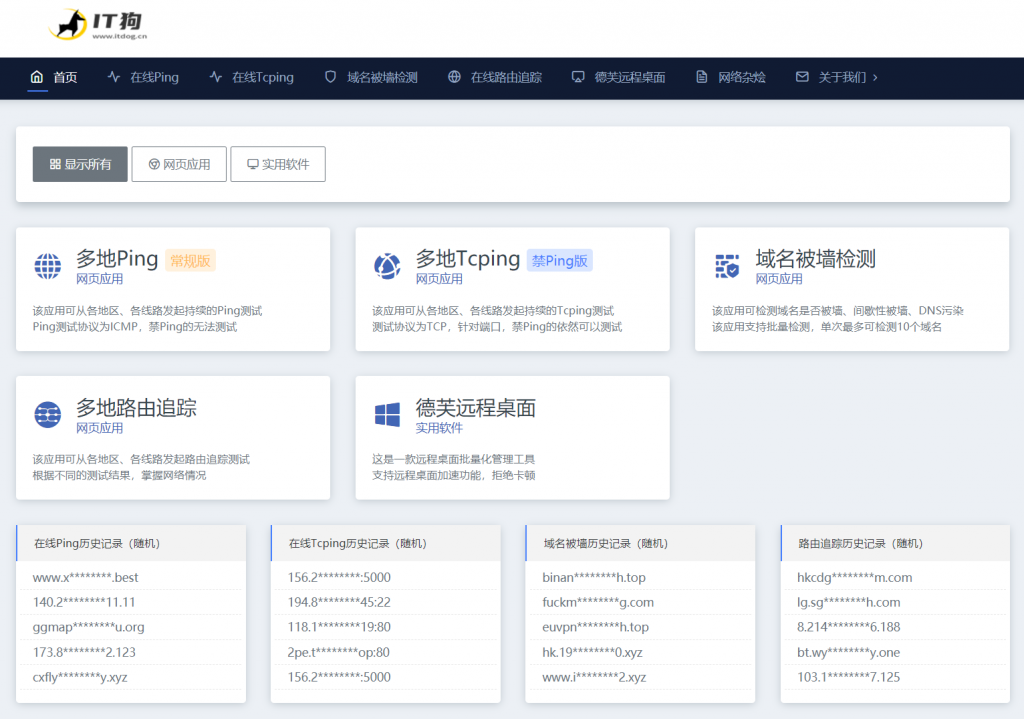
【IT狗】在线ping,在线tcping,路由追踪
IT狗为用户提供 在线ping、在线tcping、在线路由追踪、域名被墙检测、域名被污染检测 等实用工具。【工具地址】https://www.itdog.cn/【工具特色】1、目前同类网站中,在线ping 仅支持1次或少量次数的测试,无法客观的展现目标服务器一段时间的网络状况,IT狗Ping工具可持续的进行一段时间的ping测试,并生成更为直观的网络质量柱状图,让用户更容易掌握服务器在各地区、各线...
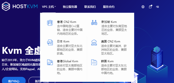
HostKvm开年促销:香港国际/美国洛杉矶VPS七折,其他机房八折
HostKvm也发布了开年促销方案,针对香港国际和美国洛杉矶两个机房的VPS主机提供7折优惠码,其他机房业务提供8折优惠码。商家成立于2013年,提供基于KVM架构的VPS主机,可选数据中心包括日本、新加坡、韩国、美国、中国香港等多个地区机房,均为国内直连或优化线路,延迟较低,适合建站或者远程办公等。下面列出几款主机配置信息。美国洛杉矶套餐:美国 US-Plan1CPU:1core内存:2GB硬盘...
www.765.com为你推荐
-
哈利波特罗恩升级当爸哈利波特最后当了当了傲罗么 ps因为在第五部里我看到他说他要当一个傲罗摩根币JPM摩根币是什么?怎么赚钱是骗人的吗?留学生认证留学生的学位证书怎样认证?留学生认证留学生回国学历认证 需要带什么材料蓝色骨头手机谁有崔健执导的电影《蓝色的骨头》。同ip网站查询我的两个网站在同一个IP下,没被百度收录,用同IP站点查询工具查询时也找不到我的网站,是何原因?地陷裂口天上顿时露出一个大窟窿地上也裂开了,一到黑幽幽的深沟可以用什么四字词语来?同ip网站12306怎么那么多同IP网站啊?这么重要的一个网站我感觉应该是超强配置的独立服务器才对啊,求高人指点百度关键词分析关键词怎么分析?www.5ff.comhttp://www.940777.com/网站,是不是真的网投六合